Lecture 9: CMOS Inverter - Part 1
 Watch on YouTube →
Overview
A CMOS inverter pairs an NMOS pull-down network with a PMOS pull-up network, and its voltage-transfer characteristic (VTC) reveals how transistor strength, switching threshold, gain, and noise tolerance shape digital logic. The lecture derives the logic threshold concept, explains how transistor sizing shifts it, and connects inverter behavior to cascading, load capacitance, noise margins, and switching-related short-circuit current.
Key takeaways
- The CMOS inverter’s switching threshold VM is the point where Vout = Vin; VM equals VDD/2 only when NMOS and PMOS strengths and threshold voltages are ideally balanced.
- Increasing NMOS width raises pull-down strength and shifts the VTC transition left, while increasing PMOS strength tends to shift it right.
- Both transistors conduct near the switching threshold, creating a temporary VDD-to-ground current path; stable logic states instead have near-zero static current apart from leakage.
- A steeper VTC transition generally improves noise immunity, and noise margins quantify the voltage gap between an output’s valid levels and the receiving stage’s input thresholds.
- Cascaded gates load an inverter through downstream MOSFET gate capacitances; parallel fan-out branches add capacitance and increase the energy and time required for transitions.
Chapters
0:00
CMOS Inverter as the Template for Digital Logic
- CMOS means complementary MOSFET: circuits use NMOS and PMOS devices in matched pull-down and pull-up networks.
- Complementary networks use the same inputs, meet at a shared output node, and often map series devices in one network to parallel devices in the other.
- The inverter is introduced as a foundational reference for comparing and designing more complex Boolean logic.
3:00
How the NMOS and PMOS Produce an Inverted Output
- With input at VDD, the NMOS conducts toward ground and the PMOS turns off, pulling the output low.
- With input at 0 V, the PMOS connects the output to VDD while the NMOS turns off, producing a high output.
- The output load capacitance charges or discharges through transistor on-resistance, so output transitions take time.
6:00
Ideal and Practical Voltage-Transfer Characteristics
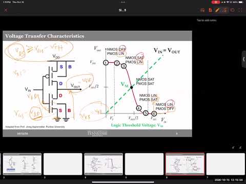
- The VTC plots output voltage against input voltage; its ideal form stays at VDD below the switching point and falls to 0 V above it.
- For a 1 V supply, VDD/2 = 0.5 V is a useful ideal dividing point between logic low and logic high.
- Practical inverters transition gradually rather than switching vertically, and a sharper VTC better approximates the ideal response.
11:00
Why NMOS and PMOS Operating Modes Change During Switching
- MOSFETs do not behave as perfect switches: their operating region depends on both gate-source voltage and drain-source voltage.
- In the long-channel model, saturation begins when VDS ≥ VGS − VT; a changing output can move either transistor between linear and saturation regions.
- The changing transistor currents across the input range produce the gradual slope in the inverter’s VTC.
19:00
Logic Threshold Voltage and the VTC Intersection
- Logic threshold voltage VM is the input level where the inverter output equals its input, found where the VTC crosses the line Vout = Vin.
- The 45-degree reference line has slope 1, so its intersection with the VTC defines the switching threshold.
- Logic groups a continuous range of voltages into low and high states, unlike analog circuits that distinguish small voltage changes.
23:00
Why Both Transistors Conduct Near the Switching Threshold
- At VM, setting Vin = Vout = VM makes the NMOS and PMOS drain and gate voltages suitable for saturation in the simplified long-channel analysis.
- Both devices conduct near the switching point, creating a temporary current path from VDD to ground.
- Equating the NMOS and PMOS currents gives an expression for VM using their device parameters; the lecture notes channel-length modulation as a refinement.
30:00
Device Balance Determines Whether VM Equals VDD/2
- The current-balance expression depends on βn and βp, which include carrier mobility, oxide capacitance, and transistor width-to-length ratio.
- VM reaches VDD/2 only in an idealized balanced case with matching NMOS and PMOS strengths and threshold voltages.
- Electron and hole mobility differ, so equal NMOS and PMOS dimensions do not generally produce equal drive strength.
37:00
NMOS and PMOS Strength Shift the Switching Point
- Increasing NMOS width increases its drive current and tends to move the VTC transition toward a lower input voltage.
- A stronger NMOS pulls the output toward ground more readily; a stronger PMOS resists that pull-down and shifts the transition in the opposite direction.
- This current-based reasoning predicts the direction of the VTC shift without requiring the full threshold-voltage equation.
42:00
Shifting the Threshold to Reject Noisy Input Fluctuations
- A noisy input can cross a fixed logic threshold repeatedly, making the output toggle and consume energy as its load capacitance charges and discharges.
- If the switching threshold is adjusted so later input fluctuations no longer cross it, the output can remain stable despite the noise.
- Inverter delay means the output cannot respond instantaneously, so rapid input fluctuations can create a particularly messy transient response.
49:00
Gate Capacitance, Cascading, and Fan-Out
- Digital logic gates are cascaded: one gate’s output commonly drives the gate terminals of one or more following transistors.
- A MOSFET gate contains an oxide-insulated structure that acts as capacitance, creating much of the load capacitance seen at the previous stage’s output.
- Fan-out adds the gate capacitances of multiple branches in parallel, increasing the load that the driving inverter must charge or discharge.
53:00
Output and Input Tolerances in Cascaded Logic
- A logic stage’s output must remain within the input-recognition range of the next stage; otherwise, a voltage intended as low or high can be misread.
- The lecture frames robust cascading as requiring conservative output levels and forgiving input tolerances.
- Noise margin expresses the voltage separation between valid output levels and the next stage’s input thresholds.
1:02:00
Noise Margins Measure Robustness to Voltage Errors
- The conventional margins are NML = VIL − VOL and NMH = VOH − VIH, where output limits are compared with the receiving input’s logic thresholds.
- A larger positive noise margin provides more tolerance to disturbances; 20 mV is safer than 10 mV under the lecture’s example.
- The flat portions of the VTC help preserve stable low and high outputs, while a near-straight, shallow response can provide little useful noise immunity.
1:06:00
Inverter Gain and the Ideal Sharp Transition
- Inverter gain is the magnitude of the VTC slope, |dVout/dVin|, evaluated around the switching region.
- A steeper transition generally supports larger noise margins; the ideal vertical transition has infinite slope in the simplified model.
- For an ideal inverter switching at VDD/2, both low and high noise margins can reach VDD/2, but real device imbalance prevents perfection.
1:09:00
Short-Circuit Current and CMOS Static-Power Advantage
- During a logic transition, NMOS and PMOS can conduct simultaneously, producing a short-circuit current spike from VDD to ground.
- At stable input levels, one transistor is off, so CMOS static current is near zero apart from leakage.
- Because switching current can be large, digital systems limit unnecessary activity; regenerative behavior is left for the next lecture.
Summary, takeaways, and chapters were generated by AI from the video's transcript and may contain errors. The video belongs to its creator, NorDIC Lab.