Lecture 8: CMOS Layout & Fabrication Process - Part 3
 Watch on YouTube →
Overview
The lecture connects lambda-based CMOS layout rules to practical stick diagrams, showing how to identify complementary NMOS/PMOS networks, wire them, and estimate their area. It also explains why modern standard-cell layouts prioritize repeatable structures and automation, then surveys how MOSFETs and metal layers can implement capacitors, resistors, and inductors before introducing emerging 3D IC transistor stacking.
Key takeaways
- In standard CMOS logic, NMOS bodies connect to ground and PMOS bodies to VDD through substrate or well taps; omitting those taps from a simplified diagram does not remove the physical requirement.
- A three-input NAND pull-down has three series NMOS transistors and a complementary pull-up with three parallel PMOS transistors; shared node labels make the connectivity easier to reconstruct.
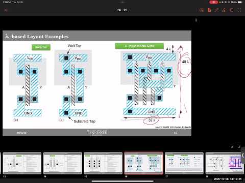
- With a 4λ minimum metal width and 4λ minimum spacing, neighboring metal-line starts are 8λ apart; the lecture's example estimates a 40λ horizontal span by counting five intervals.
- Standard-cell libraries package optimized reusable circuits, including logic gates, SRAMs, multiplexers, ADCs, and DACs, so automation tools can assemble large designs from consistent building blocks.
- MOSFETs can serve as capacitors or linear-region resistors, while on-chip inductors require cross-layer routing and are generally unattractive for digital VLSI because of their area.
- 3D IC stacking could extend integration beyond planar scaling, but the lecture describes it as an emerging process technology with unresolved manufacturing and deployment challenges.
Chapters
0:00
Cadence Files, PDKs, and the CMOS Layout Recap
- Circuit simulators such as Cadence and HSPICE generate auxiliary files; retain them because other tools may depend on them.
- Cadence Virtuoso is used across companies including NVIDIA, Intel, and TSMC, while access to advanced process design kits (PDKs) is controlled.
- The course PDK is based on an older 130 nm process; each process node has its own fabrication details and design rules.
5:15
Why CMOS Layouts Need NMOS and PMOS Body Taps
- In ordinary CMOS logic, NMOS body terminals connect to ground and PMOS body terminals connect to VDD.
- A substrate or well tap makes each body connection; bulk, body, and substrate refer to the same transistor terminal in this context.
- Body biasing can vary threshold voltage, but the lecture distinguishes it from the default fixed-body connections.
7:02
Reading a Three-Input NAND Network by Its Nodes
- Three gate signals, A, B, and C, identify three NMOS devices and three corresponding PMOS devices.
- The NMOS transistors form a series path, while naming shared nodes N1 and N2 reveals that the PMOS devices connect in parallel.
- CMOS logic uses complementary pull-down and pull-up structures: series NMOS devices correspond to parallel PMOS devices, and vice versa.
10:47
Stick Diagrams as Fast CMOS Layout Plans
- A stick diagram represents layers and connectivity with lines and simple shapes, without the exact dimensions and spacing of a physical layout.
- For a three-input gate, the diagram can show three gate lines crossing a shared NMOS diffusion path.
- Stick diagrams are suitable for paper exercises and exams; they help plan a layout before drawing it in Cadence.
16:33
Connecting CMOS Pull-Up and Pull-Down Networks
- A CMOS gate needs a connection between its PMOS and NMOS networks; the shared node becomes the output rather than leaving either network floating.
- For the illustrated three-input NAND, the PMOS side connects to VDD at one end and joins the NMOS network at the other.
- Well and substrate taps may be omitted from a simplified stick diagram, but physical layouts still need PMOS-to-VDD and NMOS-to-ground body connections.
20:23
Drawing Parallel NMOS and Series PMOS Connections
- The complementary example uses three parallel NMOS devices and three series PMOS devices, with A, B, and C controlling corresponding transistor pairs.
- Node labels such as N1 and N2 clarify which diffusion terminals must be joined and which connect to ground or VDD.
- When a same-layer route is blocked, another metal layer can cross it; the lecture notes that modern processes may provide 11 metal layers.
26:33
Why Modern Standard Cells Keep NMOS and PMOS in Separate Rows
- The lecture contrasts an older textbook layout that spreads transistors around with the modern standard-cell arrangement.
- A standard cell places NMOS devices in one region and PMOS devices in another, with VDD and ground rails arranged consistently.
- Use the structured layout taught in class for practice rather than copying the older, less standardized diagram.
27:44
Estimating Layout Area with Lambda and Metal Pitch
- Lambda is half the minimum feature size; for a 14 nm node, the stated convention gives λ = 7 nm.
- In the example, a metal line has a minimum width of 4λ and minimum spacing of 4λ, so adjacent line starts are separated by 8λ.
- Counting five 8λ intervals gives an estimated horizontal span of 40λ; the vertical estimate similarly counts required metal changes and boundary spacing.
- Stick diagrams are not to scale, so lambda-based area calculations are estimates; Cadence can measure the actual drawn layout.
38:35
Standardization Enables CMOS Design Automation
- Standardized layout patterns trade some hand-optimized compactness for consistent structures that software can place and connect.
- The lecture compares standardization to interchangeable manufactured parts: common dimensions enable repeatable production and repair.
- Automated tools rely on defined cell structures and connectivity rules rather than inventing a custom physical design for every gate.
47:07
Standard-Cell Libraries and Modular Chip Design
- Engineers optimize reusable components such as NAND gates, XOR gates, SRAMs, multiplexers, ADCs, and DACs for a standard-cell library.
- Design automation tools treat library components as reusable building blocks, much like Lego pieces, and assemble them into larger circuits.
- Modular work divides responsibility among teams, limits how much proprietary design information each person needs, and lets other work continue when one component is unfinished.
- Design automation is a major field with dedicated conferences, including DAC, Design Automation Conference.
53:12
Laying Out an Inverter Chain with Standard Cells
- A CMOS inverter pairs one NMOS and one PMOS controlled by the same input gate; their unconnected drain-side node is the output.
- Connect the NMOS source-side terminal to ground and the PMOS source-side terminal to VDD, then copy the cell to build an inverter chain.
- The first inverter's output connects to the next inverter's gate input, using a contact or via as needed to join conducting layers.
- Older diagrams show polysilicon gates; the lecture notes that contemporary transistor gates are metal.
57:25
MOSFET and Metal Structures for On-Chip Capacitors and Inductors
- A MOSFET can act as a capacitor by using its gate and body, with drain and source tied together; metal layers separated by dielectric can also form a parallel-plate capacitor.
- A metal-wire inductor can be routed as a coil, with vias connecting segments across metal layers to avoid shorting where the path crosses itself.
- On-chip inductors are generally avoided in digital VLSI because they consume substantial area; power electronics have different needs.
1:05:36
MOSFET Resistors and the Move Toward 3D ICs
- A MOSFET can operate as a resistor in its linear region; metal lines can also provide resistance, but the available metal stack is primarily designed for interconnecting transistors.
- Fringing and parallel-plate capacitor structures use metal separated by dielectric, but their spacing requirements can make them less area-efficient than MOS-based capacitance.
- As planar scaling approaches atomic dimensions, 3D IC research aims to stack transistor layers and increase integration vertically.
- Early stacked-device experiments faced process constraints—for example, a foundry trial described a second layer limited to NMOS devices—while commercial deployment still faces challenges.
Summary, takeaways, and chapters were generated by AI from the video's transcript and may contain errors. The video belongs to its creator, NorDIC Lab.