Lecture 7: CMOS Layout & Fabrication Process - Part 2
 Watch on YouTube →
Overview
The lecture connects CMOS layout conventions to the fabrication steps behind them, moving from older bulk-MOSFET process diagrams to FinFET formation and modern interconnect stacks. It explains how foundry design rules, lambda-based dimensions, alignment margins, and electromigration constraints shape transistor layouts, then applies those ideas to series and parallel NMOS connections, contact sharing, and NMOS-to-PMOS wiring.
Key takeaways
- A contact is a deliberately engineered interface: direct metal-to-semiconductor contact can behave like a Schottky diode, while contact layers are designed to support useful bidirectional current.
- Foundries set transistor threshold-voltage options through process implants; low-VT devices favor speed but increase leakage, while high-VT devices favor lower standby power.
- FinFET fabrication uses selective material removal to expose silicon fins, then places a gate around them to control the channel from multiple sides.
- Lambda-based rules express layout dimensions relative to a technology’s minimum feature size, while foundry margins account for alignment variation and reliability risks such as electromigration.
- Adjacent series transistors can share diffusion and omit a contact when their common node is internal; an external connection requires a contact and metal routing.
- Parallel devices can benefit from redundant contacts because multiple current paths reduce resistance and improve tolerance to a single contact failure.
Chapters
0:00
CMOS Inverter Layout: Gates, Contacts, and Diffusion
- The inverter layout identifies the gate, metal connections for supply, ground, and output, and N+ or P+ diffusion regions for transistor source and drain.
- A metal-to-semiconductor interface can form a Schottky diode rather than a bidirectional ohmic connection, so engineered, multilayer contacts help control the barrier.
- Modern CMOS commonly uses metal gates; older textbook layouts often depict polysilicon gates.
5:00
Photolithography and Patterning Recap
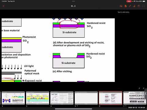
- The process begins with a silicon wafer, a thermally grown silicon-oxide layer, and photosensitive resist exposed through a patterned mask.
- Positive and negative photoresists respond differently to UV exposure, allowing selected regions to be removed before the underlying oxide is etched.
- “Patterning” compresses multiple operations—exposure, selective etching, and resist removal—often several steps for one structure.
9:00
Starting a Complementary NMOS–PMOS Fabrication Flow
- CMOS combines NMOS and PMOS devices, so the illustrated process builds both transistor types side by side.
- The older example starts with a p-type silicon substrate and an epitaxial layer; thin films can behave differently from bulk material.
- The textbook process is presented as a historical illustration, not a prescription for current foundry manufacturing.
13:00
Trench Patterning, Oxide Fill, and Well Formation
- Patterned trenches separate device regions; the diagram skips many lithography and etch operations needed to create them.
- Silicon oxide fills the trenches, and chemical-mechanical polishing (CMP) planarizes the surface.
- An N-well is implanted for the PMOS region, using the multi-step patterning and doping process introduced earlier.
17:00
Threshold-Voltage Implants and Foundry Device Flavors
- Foundries adjust threshold voltage through doping implants, making it a process-level transistor characteristic rather than a freely chosen value for every device.
- The lecture describes three common options: nominal-VT, low-VT/high-performance, and high-VT/low-standby-power devices.
- Lower VT can increase drive current and performance but also leakage; higher VT reduces current and leakage at the cost of speed.
20:00
Self-Aligned Gates, Source–Drain Regions, and Metal Contacts
- In a self-aligned process, the gate acts as a mask during source–drain doping, aligning those regions to the gate.
- The process deposits an insulating layer, opens contact holes to source and drain, and fills them with Metal 1.
- Metal 1 can connect NMOS and PMOS terminals; additional metal layers require insulating layers and vias to connect between levels.
26:00
FinFET Formation with Sacrificial Silicon–Germanium
- The illustrated FinFET flow uses patterned silicon–germanium and high-temperature oxide as intermediate materials; the silicon–germanium is later selectively removed.
- Successive deposition and etching steps expose narrow silicon fins that form the transistor channel between source and drain.
- A gate metal is deposited around the fins, giving the gate control over multiple sides of the channel.
- Material and process choices reflect foundry research and manufacturability; the exact flow varies across technology generations.
37:00
Foundries, Fabless Designers, and Multilevel Metal Routing
- The lecture contrasts fabless companies such as NVIDIA, AMD, and Qualcomm—which rely on foundries including TSMC—with Intel’s design-and-manufacturing model.
- Older 130-nanometer processes could have about six metal levels; the lecture cites roughly eleven or more for newer technologies.
- Upper metal levels are generally wider and thicker, and their vias are larger; wider conductors increase capacitance and can slow signals.
42:00
Lambda-Based Layout Rules for Metal, Diffusion, and Poly
- Foundries specify minimum widths and spacings for layout layers such as metal, diffusion, and polysilicon.
- In the lecture’s convention, lambda is half the minimum feature size; a 14-nanometer example gives λ = 7 nanometers.
- Expressing dimensions in multiples of lambda allows a layout to be rescaled by changing lambda, rather than redrawing every feature.
47:00
Why Foundry Rules Require Margins and Minimum Dimensions
- Fabrication variation can misalign a contact at a feature edge, reducing its effective area and increasing resistance; design-rule margins protect against that variation.
- Minimum metal and contact dimensions help limit electromigration, in which sustained electron flow gradually displaces metal atoms and can eventually create an open circuit.
- Margins improve reliability but consume area, so process engineers work to reduce safe minimum dimensions without sacrificing yield.
53:00
NMOS and PMOS Layout Geometry in the PDK
- A basic NMOS layout contains source, drain, gate, and source/drain contacts, with specified contact dimensions and spacing.
- PMOS geometry is similar but sits inside an N-well, which requires additional enclosure or overhang around the diffusion.
- A process design kit (PDK) packages foundry design rules into ready-to-use device cells, sparing most designers from manually rebuilding every transistor geometry.
1:00:00
Series NMOS Devices and Shared Diffusion Nodes
- Two series NMOS transistors are identified by their two gates and can share a diffusion region at their common electrical node.
- When that shared node only connects the two adjacent transistors, omitting a contact saves layout space and avoids contact-related constraints.
- If the common node must drive another circuit element, a contact and metal connection are required.
1:05:00
Parallel Devices, Redundant Contacts, and CMOS Output Wiring
- Parallel NMOS transistors have two common nodes; one can be shared in diffusion while Metal 1 connects the other terminals.
- Multiple contacts on a wider transistor provide redundancy and lower resistance, provided they fit within the existing layout footprint.
- NMOS and PMOS devices occupy separate regions, with PMOS in an N-well, so their shared inverter node must be connected through contacts and metal rather than shared diffusion.
1:10:00
Class Schedule and Upcoming Lecture Instructions
- The next class is planned as a recording because of a scheduled trip to the Quantum World Congress and other obligations.
- Students are asked to watch the recording during class time before the following meeting, where the material will be reviewed.
- An Engineering Expo was mentioned for the following Tuesday, with a possible class-time conflict and a schedule adjustment.
Summary, takeaways, and chapters were generated by AI from the video's transcript and may contain errors. The video belongs to its creator, NorDIC Lab.