Lecture 4: MOSFETS & FinFETs - Additional Concepts
 Watch on YouTube →
Overview
The lecture connects MOSFET scaling to its electrical tradeoffs: subthreshold leakage and quantum tunneling grow more consequential as devices shrink, while DIBL helped drive the shift from planar MOSFETs to FinFETs. It also explains gate-stack and threshold-voltage control, body effect, channel-length modulation, strained silicon, and why constant-voltage scaling raises reliability and power-density concerns that helped motivate multicore processors.
Key takeaways
- Subthreshold leakage is an exponential effect, so a tiny off-current per transistor can become a major power cost when billions of MOSFETs operate together.
- High-k gate dielectrics increase oxide capacitance and improve gate coupling, helping bring the MOSFET coupling factor m closer to 1.
- Short channels intensify both tunneling and DIBL: a thinner barrier raises tunneling probability, while drain voltage lowers the barrier further.
- FinFETs improve electrostatic control by wrapping the gate around three sides of a raised channel, reducing the drain's ability to control the channel.
- Body bias can trade speed for lower leakage by raising threshold voltage, and unintended source-to-body voltage can arise in series transistor stacks.
- Constant-voltage scaling increases electric-field stress and power density as device dimensions shrink, helping explain the industry shift toward multicore designs.
Chapters
0:00
Why Subthreshold Leakage Matters in VLSI
- A transistor leaks below threshold even when nominally off, and tiny leakage currents accumulate across billions of devices on a chip.
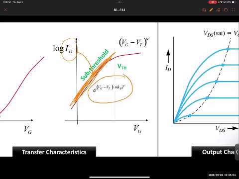
- A semi-log drain-current versus gate-voltage plot makes the rapid subthreshold current change visible.
- Below threshold, drain current depends exponentially on gate voltage and threshold voltage, unlike the roughly linear or quadratic above-threshold behavior.
4:17
From 65 nm Polysilicon Gates to 45 nm HKMG
- A 65 nm gate stack uses heavily doped polysilicon over thin silicon dioxide, with nickel silicide and strained silicon-germanium source/drain regions also mentioned.
- At 45 nm, the industry moved to high-k metal gate technology, replacing the silicon dioxide dielectric and silicon-based gate with high-k material and metal.
- The gate dielectric and semiconductor form series capacitances, so the applied gate voltage is divided between them.
7:25
Gate Coupling Factor m and Subthreshold Control
- The surface potential is approximately the applied gate voltage divided by the coupling factor m.
- For ordinary MOSFETs, m is greater than 1 because it includes a positive semiconductor-capacitance-to-oxide-capacitance contribution.
- Reducing m toward 1 improves gate control; increasing oxide capacitance, including with a high-k dielectric, reduces the relative contribution of semiconductor capacitance.
11:21
Negative Capacitance FETs and Ferroelectric Materials
- A negative capacitance element could theoretically bring m below 1 and produce surface-potential amplification.
- The lecture identifies ferroelectric materials as a route investigated for negative-capacitance transistors.
- Research groups including Berkeley, Intel, and GlobalFoundries pursued experimental negative-capacitance FETs; the topic is presented as a research area rather than standard MOSFET behavior.
12:52
MOSFET Current Equations and Quantum Tunneling
- In the simplified long-channel model, linear-region current depends roughly linearly on gate overdrive, while saturation current depends roughly on its square.
- Those equations are useful as introductory models but do not fully describe modern scaled transistors.
- Quantum tunneling gives electrons a finite probability of crossing an energy barrier without first gaining enough energy to pass over it.
17:20
Why Thinner Barriers Increase MOSFET Leakage
- The transmission probability through a barrier falls exponentially as barrier thickness increases.
- As transistor dimensions shrink, source-to-drain barriers become thinner and tunneling becomes more likely.
- Tunneling is never exactly zero; it becomes a practical leakage concern when many electrons and billions of devices are involved.
21:00
DIBL Makes Short-Channel Tunneling Worse
- A comparison of simulated 75 nm and 30 nm MOSFETs illustrates how a shorter channel reduces the separation between source and drain.
- Drain-induced barrier lowering, or DIBL, lets the drain voltage lower the source-side energy barrier, especially in short-channel devices.
- The narrower, lowered barrier raises source-to-drain tunneling and off-state leakage, making continued planar scaling increasingly difficult.
24:38
Planar MOSFETs Give Way to FinFETs
- The planar bulk MOSFET became difficult to scale as short-channel effects and tunneling increased.
- A FinFET raises the channel into a fin, allowing the gate to control it from three sides rather than only from above.
- The improved gate control suppresses drain influence and DIBL; Chenming Hu at Berkeley is credited with proposing the fin-based approach.
29:28
The Four MOSFET Terminals and Body Effect
- MOSFETs have four terminals: gate, source, drain, and body, also called the substrate or bulk.
- A source-to-body voltage can alter the channel barrier, much as gate voltage does, and therefore changes transistor behavior.
- The threshold-voltage equation includes source-to-body bias, allowing the body effect to be modeled.
32:13
Body Bias Tunes Threshold Voltage and Power
- Source-to-body voltage is a dynamically adjustable circuit knob; material parameters such as doping and oxide capacitance are not dynamically changed after fabrication.
- Increasing threshold voltage reduces both on-current and subthreshold off-current, with the off-current changing especially strongly because of its exponential dependence.
- Power-saving modes can use body bias to raise threshold voltage and reduce leakage, trading away current and operating speed.
41:13
Why Series MOSFETs Experience Body Effect
- In a series transistor stack, the shared body may be grounded while an internal source node sits at a nonzero voltage.
- The upper transistor then has a nonzero source-to-body bias even when the designer did not deliberately apply body bias.
- Different source-body voltages can give transistors in one circuit different threshold voltages, so body effect must be accounted for in circuit design.
45:03
Channel-Length Modulation and Finite Output Resistance
- In the ideal saturation model, drain current remains constant after pinch-off, but increasing drain voltage moves the pinch-off point toward the source.
- That movement shortens the effective channel and causes drain current to keep rising in saturation.
- The resulting finite output resistance is the inverse slope of the drain-current versus drain-voltage curve at fixed gate voltage; the extrapolated intercept is associated with Early voltage and the correction factor lambda.
53:56
Scaling Milestones: Strained Silicon, HKMG, and FinFETs
- Strained-silicon techniques began around the 90 nm generation, high-k metal gates around 45 nm, and FinFETs around 22 nm.
- Silicon-germanium source/drain regions create stress in adjacent silicon, changing carrier mobility and improving transistor current.
- Because hole mobility is lower than electron mobility, strain can be tuned to improve PMOS performance and reduce the need to enlarge PMOS devices to match NMOS current.
1:03:05
Constant-Field Scaling Reduces Voltage with Size
- Under constant-field scaling, device dimensions and supply voltage are reduced by the same factor, keeping electric field approximately unchanged.
- Shrinking each dimension by a factor increases the number of devices that can fit on a two-dimensional chip area.
- Lower voltage reduces power demand and avoids accelerating electric-field-driven degradation mechanisms such as time-dependent dielectric breakdown and hot-carrier injection.
1:11:17
Constant-Voltage Scaling, Reliability, and Multicore Chips
- After supply-voltage reductions stalled, geometry continued shrinking while voltage stayed roughly fixed, increasing electric fields and reliability stress.
- Constant-voltage scaling also raises power density as more transistors are packed into a chip, creating a thermal limit on larger, faster single cores.
- The lecture links this power-density challenge to the move toward multicore processors, including designs with four or eight cores instead of one increasingly powerful core.
Summary, takeaways, and chapters were generated by AI from the video's transcript and may contain errors. The video belongs to its creator, NorDIC Lab.