ECircuits-Lec24-2026
 Watch on YouTube →
Overview
The lecture derives the NMOS current-voltage equations from channel charge and carrier motion, then connects the equations to triode operation, pinch-off, and saturation. It defines the overdrive voltage, process and device transconductance parameters, and channel-length modulation, then reviews MOSFET symbols, operating-region conditions, and the distinction between DC biasing and small-signal analysis.
Key takeaways
- NMOS channel charge is controlled by gate overdrive, VOV = VGS - VTH, while drain voltage establishes a varying potential along the channel.
- The triode-region equation, ID = μnCOX(W/L)[VOVVDS - VDS²/2], becomes approximately linear in VDS when VDS is small.
- The boundary between triode and saturation is VDS = VOV; the ideal saturation current is ID = (1/2)μnCOX(W/L)VOV².
- For small drain voltage, the NMOS behaves like a voltage-controlled resistor with approximate on-resistance RON = 1/(KVOV), where K = μnCOX(W/L).
- Channel-length modulation accounts for the slight rise in saturation current as VDS increases, commonly represented by the factor 1 + λVDS.
- Operating-region checks must use both gate and drain conditions: cutoff has VGS < VTH, triode has VGS > VTH and VDS < VOV, and saturation has VGS > VTH and VDS > VOV.
Chapters
0:00
NMOS Structure, Channel Formation, and Device Dimensions
- An NMOS has an N-type source and drain in a P-type substrate; positive gate voltage attracts electrons and forms a channel.
- Positive drain voltage drives electrons from source to drain, while conventional current flows from drain to source.
- Channel length L is the source-to-drain distance; a 90 nm technology node supports a minimum channel length of 90 nm, while width W is a design choice.
4:00
Gate Overdrive Sets the Channel Charge
- The channel begins forming when VGS reaches threshold voltage VTH; the excess voltage is VOV = VGS - VTH.
- The gate oxide capacitance per unit area is COX, so the induced charge per unit area is modeled as COX times the channel overdrive.
- Multiplying charge per unit area by transistor width W gives charge per unit channel length, which can be combined with carrier velocity to calculate current.
7:00
Channel Voltage and Electron Drift Determine Current
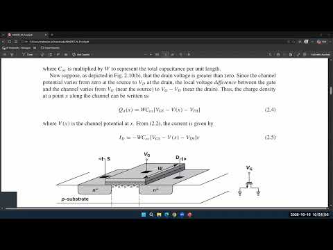
- With source voltage at 0 V and a positive drain voltage, channel voltage VX varies from 0 at the source to VDS at the drain.
- Electron drift velocity is proportional to electric field, with mobility μn as the proportionality constant and E = -dV/dx.
- Integrating the channel-current expression from x = 0 to L, while voltage varies from 0 to VDS, produces the NMOS triode-region equation.
11:00
Deriving the Triode-Region Parabola
- The integrated current is ID = μnCOX(W/L)[(VGS - VTH)VDS - VDS²/2].
- For a fixed VGS, ID varies parabolically with VDS; increasing VGS raises the curve and moves its vertex to VDS = VGS - VTH.
- For small VDS, the squared term is negligible, so current is approximately proportional to VDS.
17:00
The Parabola Vertex Marks the Saturation Boundary
- Differentiating the triode equation with respect to VDS gives the vertex at VDS = VGS - VTH, or VDS = VOV.
- At this boundary, the ideal maximum current is ID = 1/2 μnCOX(W/L)VOV².
- The parabola describes the triode region; beyond its vertex, a real MOSFET enters saturation rather than following the parabola downward.
22:00
K Parameter, Aspect Ratio, and MOSFET On-Resistance
- The aspect ratio is W/L, and the process transconductance parameter is K′ = μnCOX, which depends on the fabrication process.
- The device parameter is K = K′(W/L), giving ID = (K/2)[2VOVVDS - VDS²] in the triode region.
- For small VDS, ID ≈ KVOVVDS, so the small-voltage on-resistance is RON ≈ 1/(KVOV).
24:00
Drain-Side Depletion Causes Pinch-Off
- Positive VDS reverse-biases the drain-to-body PN junction, expanding its depletion region toward the channel.
- As VDS rises, the channel narrows near the drain, progressing from an approximately rectangular shape to a tapered shape and then pinch-off.
- Pinch-off occurs at VDS = VGS - VTH; beyond this point, the pinch-off location moves toward the source.
29:00
Saturation Current and Channel-Length Modulation
- In the ideal saturation model, ID = (K/2)VOV² and is independent of VDS once VDS exceeds VOV.
- Pinch-off shortens the effective channel from L to L′, so increasing VDS causes a small additional increase in current.
- The lecture models this non-ideal effect as ID ≈ (K/2)VOV²(1 + λVDS), where λ is the process-dependent channel-length modulation parameter.
42:00
MOSFET Symbols and LTspice Terminal Caution
- Common analog symbols show gate, source, drain, and a source arrow; some digital symbols omit the arrow, and older symbols distinguish enhancement devices with a dashed channel.
- LTspice symbols expose the bulk terminal and assign source and drain roles, so reversing those terminals can produce unexpected simulation results.
- In a physical MOSFET, source and drain roles depend on terminal voltages; the higher-potential terminal acts as the drain for the NMOS convention used here.
45:00
Cutoff, Triode, and Saturation Operating Conditions
- An NMOS is on when VGS > VTH; a positive VDS is also needed for drain-to-source conventional current.
- Cutoff occurs when VGS < VTH; triode operation requires VGS > VTH and VDS < VOV.
- Saturation requires VGS > VTH and VDS > VOV; the ideal current is controlled by VOV², with channel-length modulation adding a small VDS dependence.
- The next analysis step is DC biasing to place the MOSFET in an operating region, followed by AC small-signal analysis to determine gain.
Summary, takeaways, and chapters were generated by AI from the video's transcript and may contain errors. The video belongs to its creator, WISE Lab - UF ECE.