ECircuits-Lec21-2026 (self-study: BJT part 1)
 Watch on YouTube →
Overview
The lecture introduces BJTs by comparing their terminals and circuit behavior with MOSFETs, then derives their operation from the base–emitter diode and explains why the base must be thin. It develops the common-emitter current-gain model, distinguishes BJT operating-region terminology from MOSFET terminology, and connects the BJT exponential current equation and Early voltage to familiar MOSFET models.
Key takeaways
- A BJT’s thin base is essential: it reduces carrier recombination so most carriers injected by the emitter can reach the collector.
- A silicon BJT’s base–emitter junction is a forward-biased diode, typically modeled with V_BE near 0.7 V, while its collector current depends exponentially on V_BE through I_C ≈ I_S exp(V_BE/V_T).
- In common-emitter operation, collector current is approximately β times base current; emitter current is the sum I_E = I_C + I_B.
- The common-base gain is α = β/(1 + β), so with β = 100, α is about 0.99 rather than exactly 1.
- BJT and MOSFET saturation are not equivalent labels: MOSFET saturation describes a current region, while BJT saturation denotes operation outside the forward-active amplification region.
- BJT Early voltage V_A captures output-curve slope in a way analogous to MOSFET channel-length modulation, with V_A related to the slope parameter by V_A = 1/λ.
Chapters
0:00
Course Deadlines and Final Exam Coverage
- Homework 8 is due that night, Homework 9 is due on the 4th, and optional Homework 10 covers SPICE simulation of the Homework 8 op-amp.
- Only the best 9 of 10 homework scores count; labs should be submitted before Wednesday.
- The final is scheduled for December 10 at 10:00 a.m. in NB202, is open-book/open-notes with internet access, and lasts two hours.
- Exam review should prioritize Homework 4–9 topics, including MOSFET analysis, current mirrors, op-amp design, and digital circuits.
3:44
BJT Terminals, Polarity, and MOSFET Analogies
- BJTs come in NPN and PNP forms, with emitter, base, and collector terminals analogous to MOSFET source, gate, and drain.
- The emitter supplies carriers and the collector gathers them, while the base controls conduction.
- A MOSFET is introduced as a voltage-controlled current source; the lecture frames a BJT as a current-controlled current source, with collector current related to base current.
7:08
PN Junction Biasing and the Diode Current Equation
- A PN diode conducts strongly under forward bias and ideally blocks reverse current, apart from a small leakage current.
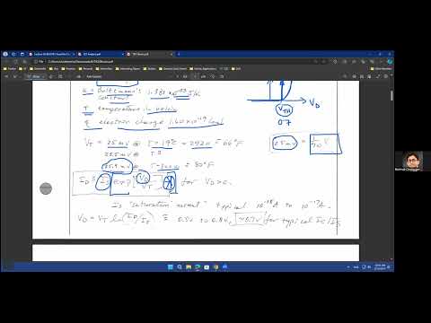
- The diode equation is approximately I_D = I_S exp(V_D/V_T); the fuller form includes the minus-one term.
- Thermal voltage is V_T = kT/q, approximately 25.9 mV at 300 K.
- The forward voltage is commonly approximated as about 0.7 V for a silicon junction; the exponential equation explains why the practical value varies with current.
18:17
Why a BJT Needs a Very Thin Base
- A BJT has emitter, base, and collector regions arranged as two adjoining PN junctions, but simply joining two ordinary diodes does not produce a useful transistor.
- In the PNP example, holes injected from the emitter can recombine with electrons in the base.
- A thin base limits recombination so that most injected carriers cross the base and reach the collector.
22:06
NPN Device Structure and Circuit Symbols
- The illustrated NPN structure places an N-type emitter and collector around a thin P-type base.
- The collector can occupy a surrounding N-type region, while the substrate connection is a fourth physical terminal often omitted in basic circuit analysis.
- The NPN symbol’s emitter arrow points outward; the terminals correspond functionally to MOSFET emitter/source, base/gate, and collector/drain.
26:12
Common-Emitter Bias and Base–Emitter Forward Conduction
- The common-emitter circuit is compared with the MOSFET common-source amplifier: the emitter is common, the input is applied at the base, and the output is taken at the collector.
- Unlike a MOSFET gate insulated by oxide, a BJT base can draw current because its base–emitter junction is a PN diode.
- For forward-biased base–emitter operation, V_BE is typically approximated as about 0.7 V, while the underlying current varies exponentially with V_BE.
30:39
BJT Operating Regions and the Saturation Naming Difference
- BJT collector-current versus collector–emitter-voltage curves resemble MOSFET output curves, but their region names differ.
- The BJT’s forward-active region is the usual region for amplification; its saturation region corresponds roughly to low collector–emitter voltage.
- MOSFET saturation describes current becoming relatively independent of drain voltage, whereas BJT saturation refers to the transistor no longer operating in forward-active mode, with carrier injection and junction biasing changing.
36:07
BJT Small-Signal Pi Model and Base Input Resistance
- The BJT small-signal pi model includes an input resistance r_π between base and emitter because base current can flow.
- Its output includes a controlled collector current represented as g_m v_be in the voltage-controlled small-signal form.
- For current-gain analysis, the same behavior can be represented as i_c = β i_b, emphasizing the relation between base input current and collector output current.
39:33
Current Gain β, α, and BJT Configurations
- In common-emitter operation, β = I_C/I_B; the lecture describes β as typically much greater than one.
- Kirchhoff’s current law gives I_E = I_C + I_B, so the common-base gain is α = I_C/I_E = β/(1 + β).
- For β = 100, α is approximately 100/101, or 0.99; unlike MOSFET drain and source currents, BJT collector and emitter currents are not exactly equal.
- Common-emitter, common-base, and common-collector BJT configurations parallel common-source, common-gate, and common-drain MOSFET configurations.
46:31
BJT Exponential Model and Early-Voltage Analogy
- The BJT collector current follows an exponential dependence on base–emitter voltage, approximately I_C = I_S exp(V_BE/V_T), rather than the MOSFET square-law model.
- The Early effect gives the BJT output curves a finite slope, analogous to MOSFET channel-length modulation.
- Early voltage V_A is the extrapolated intersection of the output curves with the voltage axis and is related to the slope parameter by V_A = 1/λ.
- The next lecture is set to apply these equations to BJT circuits and compare their behavior with MOSFET-based designs.
Summary, takeaways, and chapters were generated by AI from the video's transcript and may contain errors. The video belongs to its creator, WISE Lab - UF ECE.