ECircuits-Lec19-2026
 Watch on YouTube →
Overview
The lecture reviews four exam problems on resistor division, op-amp buffers, superposition, port resistance, and finite-gain bandwidth, including a −500 Ω transimpedance result and a closed-loop example with gain 98.3 and bandwidth about 50 kHz. It then introduces BJT operation: forward-biasing the emitter–base junction and reverse-biasing the base–collector junction lets carriers cross a very thin base, producing a large collector current relative to the base current.
Key takeaways
- Equal 10 kΩ branches split current equally, and the subsequent R5–R6 divider yields a −500 Ω transimpedance with approximately 53 dB magnitude.
- An op-amp buffer’s high input impedance removes the current-divider path into its input, allowing the full source current to flow through the remaining resistor branch.
- With A0 = 10,000 and a 5 MHz gain-bandwidth product, the open-loop bandwidth is 500 Hz; feedback raises the example’s closed-loop bandwidth to about 50 kHz while preserving a gain near 98.3.
- A BJT’s emitter–base junction is forward biased and its base–collector junction reverse biased; the base must be thin so most injected carriers reach the collector.
- For a BJT, IE = IC + IB; a small base current can control a much larger collector current because only a minority of injected carriers return through the base.
- In common-base configuration, the base is shared, the emitter is the input, and the collector is the output; the input curve resembles a diode while the output curve is a distinct collector-current-versus-voltage characteristic.
Chapters
0:00
Exam Question 1: Resistor Reduction and −500 Ω Transimpedance
- The source is a current input and the output is a voltage, so the transfer function is transimpedance, measured in ohms.
- Combining R3 = 10 kΩ in parallel with R4 = 10 kΩ, then in series with R2 = 5 kΩ, gives a 10 kΩ branch; R5 + R6 also equals 10 kΩ.
- Equal 10 kΩ branches split the source current equally, and the R5–R6 divider produces a reported transimpedance of −500 Ω.
- The negative sign denotes polarity inversion; the magnitude corresponds to about 53 dB using 20 log10(500).
3:47
Exam Question 2: A Unity-Gain Buffer Prevents Current Division
- A unity-gain buffer connects the signal to the op-amp’s non-inverting input and feeds the output back to its inverting input.
- With ideal infinite input impedance, no current enters the op-amp input, so the source current does not divide into the buffer-side branch.
- The full current flows through the remaining 10 kΩ path, and the buffer reproduces that node voltage at its output.
- The exam solution reports a transimpedance of −10 kΩ, or roughly 80 dB in magnitude; the key circuit distinction is the absence of input current.
7:22
Exam Question 3: Superposition and Port Resistance
- For the two-source op-amp circuit, superposition analyzes each source separately while replacing the other ideal voltage source with a short to ground.
- The two output contributions are 100(VS/2) and 99(VS/2), which add to an overall gain of approximately 99.5.
- To find input resistance, remove the original sources and apply a test voltage across the specified input port; the ideal op-amp input draws zero current, giving infinite input resistance.
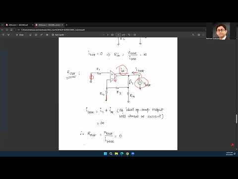
- To find output resistance, short the independent input sources and apply a test source at the output; the ideal op-amp output path gives zero output resistance.
12:00
Exam Question 4: Finite Op-Amp Gain and Closed-Loop Bandwidth
- The non-ideal op-amp has open-loop gain A0 = 10,000 and gain-bandwidth product A0f0 = 5 MHz, giving an open-loop bandwidth of 500 Hz.
- The feedback factor is approximately β = 0.008; with the ideal closed-loop gain near 99.5, finite open-loop gain reduces the result to about 98.3.
- Using the 5 MHz gain-bandwidth product and closed-loop gain of 98.3 gives a closed-loop bandwidth of approximately 50 kHz.
- The equivalent approximations fCL ≈ (1 + T)f0 and fCL ≈ β·GBW provide alternative ways to estimate closed-loop bandwidth.
15:23
Port Definitions and Test-Source Setup
- A resistance measurement applies a test source across a two-terminal port, with port current entering one terminal and returning through the other.
- When calculating resistance, independent voltage sources are deactivated by shorting them before the test source is connected.
- The explanation emphasizes identifying both port terminals and tracing the test current rather than choosing an arbitrary reference node.
19:20
Virtual Ground: Why Op-Amp Inputs Share Nearly the Same Voltage
- Negative feedback and high open-loop gain drive the differential input voltage close to zero; the virtual-ground condition is a consequence of this behavior, not an actual ground connection.
- With one source active, the non-inverting input can sit at VS/2, so the inverting input is also approximately VS/2.
- A voltage across R2 still drives current through it; because the op-amp input ideally draws no current, that current must come through the surrounding resistor network.
- For a finite-gain op-amp, the input terminals are only approximately equal in voltage, with the error depending on the open-loop gain.
26:40
BJT Structure, Carrier Types, and Forward/Reverse Bias
- A BJT contains two semiconductor junctions in a PNP or NPN arrangement and has emitter, base, and collector terminals.
- An NPN emitter is N-type and injects electrons; a PNP emitter is P-type and injects holes.
- For normal carrier transport, the emitter–base junction is forward biased and the base–collector junction is reverse biased.
- The emitter supplies majority carriers and the collector attracts and collects them, with battery polarity selected to support that transport direction.
33:30
The Thin BJT Base Lets Carriers Reach the Collector
- A BJT’s base is made extremely thin compared with its emitter and collector; the lecture illustrates a 1 mm emitter and collector with a 1 μm base.
- Forward bias injects carriers from the emitter into the base, and the reverse-biased collector junction sweeps most across the thin base.
- Some carriers recombine or return through the base, so transport is not complete; the large fraction reaching the collector creates unequal collector and base currents.
- The emitter and collector roles depend on biasing: the forward-biased side acts as the emitter, while the reverse-biased side acts as the collector.
41:50
BJT Current Gain Comes from Emitter–Collector Asymmetry
- Kirchhoff’s current law gives IE = IC + IB for either PNP or NPN transistors when currents are treated with consistent directions.
- The example uses IE = 1.001 mA, IC = 1 mA, and IB = 0.001 mA to show that base current can be much smaller than collector current.
- If a small varying base current changes, the much larger collector current changes correspondingly, providing the basis for BJT current amplification.
- Amplification depends on the thin-base asymmetry: most injected carriers reach the collector, while a smaller portion contributes to base current.
45:20
Common-Base Configuration and Its Input/Output Characteristics
- A BJT has three basic amplifier configurations—common base, common emitter, and common collector—named for the terminal shared by input and output.
- In common-base operation, the base is the shared reference, the emitter is the input, and the collector is the output.
- The input characteristic plots emitter current against base–emitter voltage and resembles a forward-biased diode because the emitter–base junction is a diode junction.
- The output characteristic plots collector current against collector-side output voltage; its behavior differs from a simple diode and is developed in the following lecture.
Summary, takeaways, and chapters were generated by AI from the video's transcript and may contain errors. The video belongs to its creator, WISE Lab - UF ECE.