ECircuits-Lec18-2026
 Watch on YouTube →
Overview
The lecture resolves Exam 1 questions on resistor values, superposition, input resistance, and nonideal op-amp gain, then explains diode clipper and clamper circuits and diode-capacitor voltage multipliers. It derives how diode polarity and bias set clipping or clamping levels, how capacitor charging and discharge time constants shape clamper behavior, and how a voltage doubler can produce approximately 2VM, with real-world output limited by diode leakage and load current.
Key takeaways
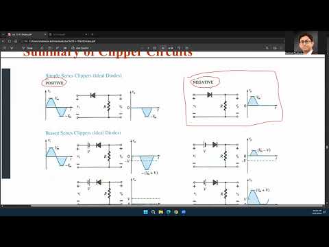
- An ideal diode's bias state determines whether a clipper passes or suppresses a waveform segment; adding a DC source shifts the threshold, such as moving it to ±5 V with a 5 V bias.
- A clamper preserves the input waveform but shifts its DC level: a capacitor charged to V during one half-cycle can combine with the next −V input half-cycle to produce an approximately −2V output.
- A clamper needs asymmetric time-constant behavior: the diode path should charge the capacitor quickly, while the discharge time constant should be much longer than a waveform half-period.
- In the illustrated voltage doubler, C1 charges to approximately VM and the next half-cycle adds the source's VM to that stored voltage, charging C2 to approximately 2VM.
- Voltage-multiplier output is limited by nonideal diode leakage and load discharge; adding stages increases the ideal voltage but does not permit unlimited voltage from a finite input.
- For Exam 1's two-source op-amp circuit, superposition is a straightforward method, but another valid analysis method is acceptable if source polarity and the requested quantity are handled correctly.
Chapters
0:00
Exam 1 Clarifications: Resistors, Superposition, and Op-Amp Gain
- Exam 1 is due that night; the stated values are R1 = 10 kΩ, R2 = 5 kΩ, R3 = R4 = 10 kΩ, R5 = 9 kΩ, and R6 = 1 kΩ.
- Question 2 uses an op-amp open-loop gain of 100 V/V; decibel gain is not required unless explicitly requested.
- For Question 3, superposition can isolate the two sources, but nodal analysis or another correct method is also acceptable; track source polarities at the op-amp inputs.
- For Question 4, find the feedback factor β and closed-loop gain, then use the op-amp gain-bandwidth relationship to determine closed-loop bandwidth.
5:17
Series Diode Clippers and DC-Biased Thresholds
- A series clipper removes the half-cycle in which its diode is reverse-biased; an ideal diode acts as a short when forward-biased and an open when reverse-biased.
- Adding a 5 V battery shifts the diode's turn-on threshold, so an input threshold can move to −5 V or +5 V depending on battery polarity.
- For the illustrated biased series clipper, draw the threshold line first, then determine which portion of the input waveform reaches the output.
- The half-wave rectifier is a series clipper: reversing the diode changes which half-cycle passes and the polarity of the resulting rectified output.
9:39
Parallel Clippers: Output Across the Shunt Diode
- A parallel, or shunt, clipper places the diode on a path to the reference node; when forward-biased, it clamps the output across the diode to approximately 0 V in the ideal model.
- When the diode is reverse-biased, the branch is open; with no current through the series resistor, the output can follow the input.
- Reversing the diode changes which input half-cycle is clamped, while adding a DC bias shifts the conduction threshold.
- Analyze each configuration by identifying the diode's bias state and the voltage across the output terminals in both states.
15:02
Biased Parallel Clippers and Shifted Conduction Regions
- A battery in a parallel clipper shifts the voltage at which the diode begins conducting, producing output transitions at a bias-dependent threshold.
- When the diode conducts, its ideal short circuit makes the output equal to the bias-source voltage; when it is off, the output follows the input relative to the shifted threshold.
- The waveform can therefore contain a flat segment at the bias level as well as an input-following segment.
- Series and parallel clippers can each be positive, negative, or biased; diode orientation and source polarity determine the result.
19:23
Clamper Circuits Shift the Entire Waveform
- Unlike a clipper, a clamper retains the complete input waveform but shifts its DC level so a maximum or minimum is fixed to a reference voltage.
- The example shifts a waveform down by V: its positive peak moves to 0 V and its negative peak to −2V.
- A capacitor added to the diode-resistor network stores charge during one half-cycle and supplies the voltage offset during the other.
- Clamping performance depends on choosing the capacitor and resistance so the waveform passes while the stored charge is retained.
22:10
Clamper Operation: Capacitor Charging and the 2V Output
- During the positive half-cycle, the forward-biased diode acts as a short, the output is approximately 0 V, and the capacitor charges to V.
- During the negative half-cycle, the diode is reverse-biased and the source voltage adds to the stored capacitor voltage, producing an output of approximately −2V.
- The capacitor voltage cannot change instantaneously; in practice, its charging and discharge paths determine how closely the output approaches the ideal waveform.
- The diode's forward path should charge the capacitor quickly, while a large effective discharge resistance keeps the RC time constant much longer than the waveform half-period.
33:22
Biased Clampers Set a Chosen Waveform Limit
- A DC source added to a clamper sets the waveform's clamp level; the illustrated 10 V bias shifts the waveform so its minimum is held at −10 V.
- The direction of the diode and bias source determines whether the circuit clamps a maximum or a minimum.
- The input waveform keeps its shape in the ideal case, while the bias determines its DC shift.
35:21
Voltage Doubler: Charging Capacitors to VM and 2VM
- A transformer can isolate the input from the multiplier and set the secondary voltage; VM denotes the secondary peak voltage.
- In the first half-cycle, D1 conducts and C1 charges to approximately VM; in the opposite half-cycle, D1 turns off and D2 conducts.
- The source's VM and the stored VM across C1 add in the second charging loop, allowing C2 to charge to approximately 2VM.
- The output across C2 is a DC voltage whose sign depends on the chosen output-terminal polarity; a connected load can discharge the capacitor.
48:00
Cascaded Voltage Multipliers, Leakage, and Energy Harvesting
- Adding diode-capacitor stages extends a voltage doubler into tripler and quadrupler circuits, with each stage contributing to the output voltage.
- Real diode leakage and finite resistance limit how far capacitors can charge, so voltage multiplication cannot produce unlimited output from a small input.
- Load current sets the discharge rate: a high-resistance, low-current load preserves capacitor voltage better than a low-resistance load.
- Voltage multipliers can support energy-harvesting systems that convert small AC inputs, such as tens of millivolts, into higher DC supplies, subject to leakage and load limits.
50:29
BJT Preview: Two PN Junctions and Three Terminals
- The next topic is the bipolar junction transistor, formed from two PN junctions connected back to back.
- NPN and PNP structures add a third terminal compared with the two-terminal PN diode.
- The lecture previews how the two junctions and three semiconductor regions enable transistor applications.
Summary, takeaways, and chapters were generated by AI from the video's transcript and may contain errors. The video belongs to its creator, WISE Lab - UF ECE.