Lecture 3 SRAM Part 5
 Watch on YouTube →
Overview
Shimeng Yu explains how manufacturing variation, aging, and radiation affect SRAM reliability, then traces transistor scaling from planar MOSFETs through FinFETs to gate-all-around nanosheets. Key quantitative examples include 1–2 nm line-edge roughness, a 3 nm high-k layer with 0.7 nm of interfacial oxide yielding 1.2 nm EOT, and a FinFET effective width of 2Hfin + Tfin; the lecture concludes with backside power delivery, CFETs, and 3D cache integration.
Key takeaways
- At a 15–16 nm gate length, 1–2 nm of line-edge roughness can represent roughly 10% channel-length variation, materially affecting threshold voltage and leakage.
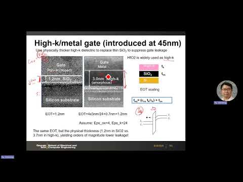
- A 3 nm hafnium-oxide layer plus a 0.7 nm SiO₂ interfacial layer can provide about 1.2 nm EOT while retaining a thicker physical tunneling barrier.
- SRAM soft-error risk depends on collected charge exceeding critical charge; scaling reduces both sensitive junction area and capacitance, but increases the number of vulnerable bits per chip.
- FinFET gate control improves short-channel behavior, but integer fin counts constrain sizing; nanosheets recover width flexibility through selectable sheet dimensions and stronger four-sided gate control.
- Backside power delivery separates power and signal routing to ease congestion, but moves the transistor layer farther from the heat sink and creates a significant thermal-design tradeoff.
Chapters
0:00
Line-Edge Roughness Becomes Significant at 15 nm Gate Lengths
- Lithography leaves photoresist edges rough because exposure and development remove discrete polymer molecules unpredictably.
- Typical line-edge roughness is about 1–2 nm sigma, or roughly 5 nm at three sigma.
- A 1–2 nm channel-length change is a small fraction of a 100 nm device but around 10% of a 15–16 nm gate, affecting threshold voltage and leakage.
4:00
High-k Metal Gates Preserve Capacitance While Limiting Tunneling
- Shrinking SiO₂ below roughly 1 nm raises direct-tunneling gate leakage, so advanced CMOS adopted high-k dielectrics and metal gates from the 45 nm generation onward.
- Hafnium oxide has roughly five to six times the dielectric constant of SiO₂, allowing a physically thicker gate dielectric while maintaining or increasing gate capacitance.
- A 3 nm high-k layer with a dielectric-constant ratio of 4:24 contributes about 0.5 nm EOT; adding a 0.7 nm SiO₂ interfacial layer gives about 1.2 nm total EOT.
10:25
Metal Work-Function Variation Adds Threshold-Voltage Spread
- Metal-gate work function helps set transistor threshold voltage and supports foundry offerings such as low-, standard-, and high-VT devices.
- Grain structure, alloy composition, and metal thickness can vary locally, producing transistor-to-transistor work-function and VT variation.
- For nanosheet gates with limited space to adjust metal thickness, interface dipoles and fixed charges provide another VT-tuning method, but their quantities are also difficult to control precisely.
14:15
Random Telegraph Noise and BTI Shift Transistor Behavior Over Time
- Random telegraph noise occurs when an oxide or interface trap captures and releases an electron, producing discrete current or apparent VT changes in a short-channel transistor.
- A small subset of devices can show RTN shifts with tails reaching about 50–60 mV; multiple traps can make the variation appear smoother.
- Bias temperature instability is an aging effect: elevated gate stress and temperature accelerate VT drift, so SRAM noise margins must account for years of operation, not only fresh-device measurements.
21:00
Cosmic-Ray Strikes Cause SRAM Soft Errors
- Energetic particles can generate electron-hole pairs in silicon; charge separation near a reverse-biased junction creates a transient photocurrent.
- If the collected charge exceeds the cell's critical charge, the current can discharge a stored node and flip its logic state; rewriting or error correction can recover a soft error.
- With scaling, the sensitive junction area and critical charge both shrink, leaving cell-level upset probability broadly comparable while the greater number of SRAM bits raises system-level exposure.
- DRAM cell capacitance is deliberately added and changes less with scaling, so a shrinking sensitive junction can improve cell-level soft-error immunity relative to SRAM.
32:00
Parasitic Bipolar Action Can Turn One Strike into Multiple Bit Upsets
- A strike can raise local substrate or well voltage because hole current must flow through the resistance to a shared body contact at the array edge.
- If that voltage activates a parasitic bipolar transistor, current can discharge a neighboring cell's stored-one node and propagate a multi-bit upset.
- Closer SRAM cells in scaled arrays increase the risk of adjacent upsets, motivating error-correcting codes that can handle multiple-bit errors.
38:10
SOI Reduces Radiation Sensitivity Before the FinFET Transition
- Silicon-on-insulator places a thin silicon layer over buried oxide, reducing the junction volume involved in charge collection and offering a technology-level radiation-hardening option.
- SOI platforms are available from foundries for applications requiring radiation tolerance, but can cost more than bulk silicon at a comparable node.
- The lecture then introduces FinFETs as the move away from planar bulk transistors for leading-edge short-channel control.
45:00
FinFET Geometry Raises Effective Width Above Its Footprint
- A FinFET channel is a vertical silicon fin controlled on its two sidewalls and top surface, giving effective width W = 2 × fin height + fin thickness.
- In the Intel example, a 34 nm fin height and 8 nm fin thickness yield about 76 nm effective width per fin.
- The example's contact or poly pitch is about 90 nm; Berkeley research appeared in 1998, and Intel commercialized FinFETs in its 22 nm platform in 2012.
51:40
Fin Quantization Trades Flexible Sizing for Higher Drive
- A FinFET transistor uses an integer number of fins, so its effective width changes in discrete steps rather than allowing arbitrary planar width choices.
- Seven fins at 76 nm effective width each provide about 532 nm of effective electrical width, even if their physical layout footprint is narrower.
- Three-sided gate control couples more strongly to the channel than a planar top gate, improving subthreshold behavior and reducing short-channel effects and drain-induced barrier lowering.
55:50
SRAM Fin Counts Set Pull-Up, Pull-Down, and Pass-Gate Ratios
- In FinFET SRAM layouts, designers set the pull-up, pull-down, and pass-gate strength ratio by assigning integer fin counts.
- The 22 nm high-density cell example uses a 1:1:1 ratio, while a higher-drive example uses two pull-down fins and one fin each for pull-up and pass-gate devices.
- L1 cache favors larger, faster cells with more fins; L3 cache prioritizes density and can use the 1:1:1 configuration.
1:00:55
FinFET Scaling Combines Tighter Pitch with Taller Fins
- From Intel's 22 nm to 14 nm generation, the lecture cites roughly 50% SRAM area reduction, while later SRAM scaling becomes increasingly difficult below 7 nm.
- Fin pitch shrinks to improve density, while fin height increases to raise effective width and drive current.
- Fin width changes less because the fins are already only a few nanometers thick; TSMC's 5 nm generation introduced silicon-germanium in PMOS fins to improve hole mobility.
1:06:20
Undoped Fin Channels Shift Variation Toward Edge Roughness
- Leading-edge FinFET channels are typically undoped, making random dopant fluctuation far less important than in earlier planar devices.
- Source/drain doping and metal-gate work function distinguish NMOS and PMOS behavior and help set threshold voltage.
- When a fin is only about 6–8 nm wide, 1–2 nm edge roughness becomes a large fraction of its dimensions and can dominate device variation.
1:10:45
Nanosheets Restore Width Flexibility with Gate-All-Around Control
- At leading-edge nodes, SRAM bitcell area is described as having largely plateaued; the cited high-density cell area is about 0.021 μm², comparable across recent generations.
- Nanosheet transistors stack thin horizontal silicon channels and surround each channel on four sides with a gate, strengthening electrostatic control beyond the three-sided FinFET.
- For each sheet, effective width is approximately 2 × sheet width + 2 × sheet thickness; stacking sheets and choosing their width restores more flexible transistor sizing than integer fin counts.
1:13:45
Nanosheet Dipole Engineering and Backside Power Delivery
- Nanosheet fabrication stacks silicon and silicon-germanium layers, patterns them, then removes sacrificial SiGe to release silicon channels between source and drain.
- Fixed-volume nanosheet gates limit work-function tuning by metal thickness, increasing reliance on interface dipole engineering; the channel orientation can also disadvantage PMOS mobility.
- Backside power delivery moves VDD and VSS routing away from frontside signal metal, reducing routing congestion and potentially shrinking standard-cell height.
- Intel's 18A process is described as using backside power delivery, while TSMC's A16 plan includes it; thermal management remains a key challenge.
1:16:15
CFETs and 3D Cache Integration Point to Future SRAM Designs
- Backside power delivery complicates heat removal because the transistor layer is less directly coupled to the heat sink through the thermally conductive silicon substrate.
- Complementary FETs (CFETs) stack NMOS and PMOS vertically; folding SRAM layouts this way could free area and create renewed scaling opportunities in a later generation.
- Design-technology co-optimization links circuit and process choices, while AMD accelerator examples illustrate heterogeneous integration of cache, I/O, and compute dies.
- Placing compute dies above cache can keep hot CPU or GPU logic closer to the top-side heat spreader, with SRAM/cache layers positioned below.
Summary, takeaways, and chapters were generated by AI from the video's transcript and may contain errors. The video belongs to its creator, Shimeng Yu.