Lecture 3 SRAM Part 4
 Watch on YouTube →
Overview
Shimeng Yu explains why modern six-transistor SRAM layouts favor a wide, mostly rectilinear design over older tall layouts, and how foundry-specific push-rule design and lithography techniques make dense patterns manufacturable. He then connects SRAM scaling limits to transistor variability: cell area reaches roughly 0.02 µm² at advanced nodes, while threshold-voltage mismatch narrows read noise margins, with random dopant fluctuation as one important source in bulk CMOS.
Key takeaways
- Modern six-transistor SRAM cells favor a wide layout with aligned gates and mostly straight features because it is easier to pattern than older tall layouts with T-shaped routing and mixed gate orientations.
- Foundry-qualified push-rule design can shrink SRAM layouts beyond standard logic design-rule limits, but designers cannot safely apply those rule violations without process-integration validation.
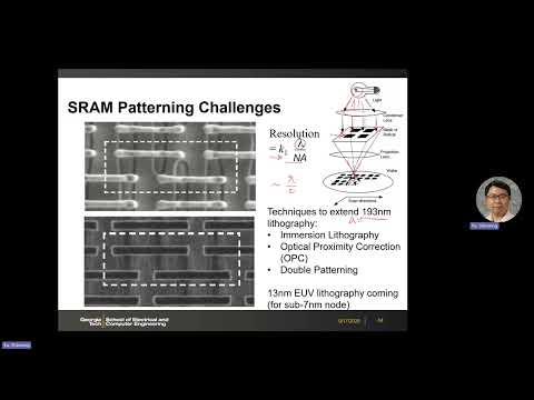
- For sub-193 nm features, manufacturers combine immersion lithography and OPC with multiple-patterning methods; EUV at about 13.5 nm supports leading-edge processes.
- SRAM cell-area scaling has flattened: the lecture cites about 0.1 µm² at 22 nm and roughly 0.02 µm² for high-density cells at advanced nodes, with array density near 38 Mb/mm² including peripheral circuits.
- Threshold-voltage mismatch makes SRAM butterfly curves asymmetric and reduces read noise margin, making variability a direct constraint on reliable array operation.
- In scaled bulk CMOS, RDF grows more consequential as the channel contains fewer dopants; dopant placement as well as count can create leakage paths, while other mechanisms explain variation beyond the RDF model.
Chapters
0:00
Why Modern SRAM Uses Wide, Straight-Patterned Cells
- Older SRAM layouts used a tall-cell arrangement; modern designs below roughly the 90 nm era commonly use a wide-cell arrangement.
- The older layout contains T-shaped storage-node routing and differently oriented transistor gates, making its patterns harder to print at small dimensions.
- Modern wide cells align transistor gates in the same direction and favor horizontal and vertical features, improving lithographic patternability.
5:11
Foundry Push-Rule Design for Compact SRAM Cells
- A designer following standard logic-process design rules may not be able to shrink a six-transistor SRAM cell to its minimum dimensions.
- Foundries can collaborate with process-integration teams to create SRAM-specific push-rule layouts that intentionally depart from some logic design rules.
- These custom dimensions require foundry qualification; using them without the fabrication partner's validation provides no manufacturing guarantee.
8:38
193 nm Lithography, Immersion, and Optical Proximity Correction
- A GDS layout is transferred through a photomask and optical system onto photoresist, which then patterns underlying materials such as metal or isolation layers.
- Conventional 193 nm lithography faces a resolution limit on the order of half the wavelength; immersion lithography increases numerical aperture by placing liquid in the optical path.
- Optical proximity correction (OPC) alters mask shapes to compensate for diffraction and other exposure distortions, helping fabricated features match the intended GDS geometry.
15:48
EUV and Multiple Patterning for Sub-193 nm Features
- Extreme ultraviolet lithography uses a wavelength of about 13.5 nm and is used for leading-edge logic and DRAM; ASML is identified as the sole supplier of EUV scanners.
- Before EUV, processes such as 16 nm and 12 nm relied on double patterning because 193 nm immersion lithography could not print the required features in one exposure.
- A pattern can be split into simpler steps—for example, first printing parallel stripes and then using a separate cut mask to define final shapes.
- Sidewall-transfer techniques can use deposited sidewall material as a hard mask to produce narrow features, including very thin fins.
20:14
SRAM Cell-Area Scaling and the Modern Density Plateau
- At the 22 nm technology node, the six-transistor SRAM cell area is approximately 0.1 µm², following a strong historical scaling trend.
- At advanced nodes, including 5 nm, 3 nm, and 2 nm labels, high-density six-transistor cells are around 0.02 µm² rather than continuing to shrink proportionally.
- Including peripheral circuits such as sense amplifiers and decoders, reported array density is about 38 Mb/mm² for processes such as TSMC N20 and Intel 18A.
24:32
How Transistor Mismatch Shrinks SRAM Read Noise Margin
- Ideal SRAM butterfly curves have symmetric left and right branches, but transistor threshold-voltage mismatch makes the branches unequal and reduces one side's noise margin.
- At array scale, designers must consider a distribution of butterfly curves and the resulting narrow read-stability window, which becomes more challenging as process variability increases.
- The lecture identifies random dopant fluctuation (RDF), line-edge roughness (LER), and metal-gate work-function variation as spatial sources of transistor mismatch.
- Random telegraph noise (RTN) and bias-temperature instability (BTI) are temporal sources that can change a transistor's threshold voltage over time.
30:16
Random Dopant Fluctuation and Threshold-Voltage Spread
- In bulk CMOS, random dopant fluctuation becomes significant as channel dimensions shrink: when a channel contains only about 100 dopants, a difference of one or two dopants can materially change the local concentration.
- Both dopant count and dopant placement affect threshold voltage; uneven placement can leave a weakly blocked path through the channel, increasing leakage and lowering the effective threshold.
- The empirical RDF contribution to threshold-voltage spread scales approximately with the inverse square root of gate area, so smaller gate areas produce greater variation.
- For scaled channels around a few tens of nanometers, the lecture cites fewer than 100 channel dopants and possible one-sigma VTH variation of 60–70 mV; deviations from the RDF trend indicate additional variability sources.
Summary, takeaways, and chapters were generated by AI from the video's transcript and may contain errors. The video belongs to its creator, Shimeng Yu.