Lecture 3 SRAM Part 3
 Watch on YouTube →
Overview
Shimeng Yu explains how SRAM designers manage the read/write stability conflict in scaled 6T cells, comparing voltage-assist methods with 8T read-decoupled and dual-port designs. The lecture then connects transient stability and Shmoo measurements to speed, leakage, interconnect, and layout, including 65 nm and 5 nm operating examples and an estimated 160 F² 6T cell layout.
Key takeaways
- A conventional 6T SRAM cell has an inherent read/write sizing conflict: reads favor a strong pull-down and weak pass gate, while writes favor a strong pass gate relative to the pull-up.
- An 8T read-decoupled cell uses two additional transistors to isolate the read path, allowing read noise margin to approach hold noise margin at the cost of cell area.
- SRAM stability is dynamic as well as static: whether a cell flips depends on disturbance duration and the integrated charge, not voltage amplitude alone.
- In a Shmoo plot, low-voltage failures are commonly read-limited, while high-frequency failures are commonly write-limited because short pulses cannot deliver enough charge.
- A 6T cell typically has three off-state leakage contributors, and aggregate cache leakage can reach milliwatt scale even when the array is idle.
- The illustrated layout estimate is about 160 F², based on dimensions of roughly 8F by 20F and a 2:1:1 pull-down/pass-gate/pull-up sizing ratio.
Chapters
0:00
Why 6T SRAM Read Stability Conflicts with Writeability
- As SRAM cells scale, the read butterfly curve and static noise margin shrink.
- During a read, the pass gate should be weak and the pull-down transistor strong to avoid disturbing stored data.
- During a write, the pass gate must overpower the pull-up transistor to change the stored value.
- Because read and write share the 6T cell's pass gate, their sizing requirements conflict.
4:00
Wordline Underdrive and Voltage Assist for SRAM Reads and Writes
- Read assist can underdrive the wordline below the cell supply, weakening the pass gate without changing transistor dimensions.
- Lowering the wordline by about 100 mV improves read static noise margin by roughly 50 mV in the example.
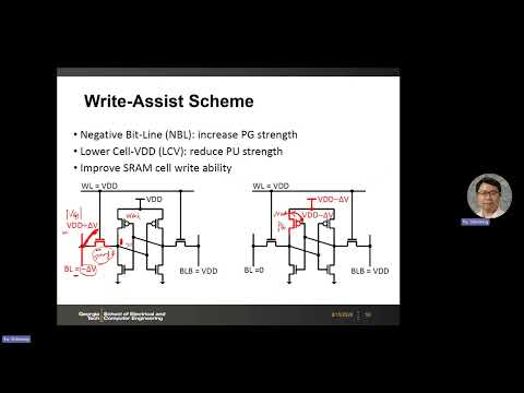
- Write assist can raise bitline voltage to increase pass-gate VGS, or lower cell supply to weaken the pull-up.
- Voltage assists are especially useful in minimum-sized cells, where NMOS and PMOS mobility differences provide less sizing advantage.
10:45
Multiple SRAM Supply Domains and Read-Modify-Write for Masked Columns
- A memory can use separate supplies for the SRAM core and peripheral circuits; peripheral VDD can often be reduced more aggressively than cell VDD.
- In a 128-column example that writes only 8 bits, unselected columns can be disturbed by a write pulse intended for selected columns.
- Read-modify-write first reads and buffers the full row, replaces selected bits with new input data, then writes the row back.
- The buffered old values preserve unselected columns while selected columns receive new data.
16:20
8T SRAM Separates the Read Port from the Write Port
- The 8T read-decoupled cell adds two transistors to form a read path separate from the conventional 6T write path.
- During a read, the stored value controls a series transistor pair that either discharges the precharged read bitline or leaves it high.
- Because the read path does not disturb the storage nodes, read noise margin can match the cell's hold condition.
- The extra two transistors cost cell area but support more aggressive supply-voltage reduction with improved read stability.
20:20
Dual-Port 8T SRAM Enables Concurrent Operations on Different Rows
- A different 8T design adds separate read and write pass-gate pairs controlled by distinct wordlines.
- It permits one row to be read while a different row is written, increasing array-level bandwidth.
- Read and write are not intended to occur simultaneously in the same cell.
- Yu notes this organization is useful in bandwidth-intensive designs such as some GPU caches.
24:00
Transient SRAM Stability: Current Injection and Recovery Trajectories
- Dynamic stability models a finite-duration disturbance rather than assuming noise persists indefinitely, as static analysis does.
- A current pulse injected into a storage node charges its parasitic capacitance, changing the two storage-node voltages over time.
- If the pulse ends before the trajectory crosses the stability boundary, the cross-coupled latch restores the original data.
- If the disturbance lasts long enough to cross the boundary, the latch switches to the opposite stable state.
31:00
Critical Disturbance Time and Charge for SRAM Switching
- For a given injected current, the critical time marks when the storage-node trajectory crosses into the other stable state.
- The relevant physical quantity is critical charge: the time integral of current into or out of the storage node.
- Read and hold disturbances should end before crossover; a write pulse must last long enough to cause crossover.
- A write may pass a static voltage-margin test yet fail dynamically if its pulse is too short to deliver the required charge.
37:00
Why Static Noise Margin Is Pessimistic for Reads but Optimistic for Writes
- Static read and hold analysis assumes a disturbance remains indefinitely, so it can predict failure for a voltage pulse that is harmless when brief.
- For example, a 300 mV disturbance lasting 100 ps may be tolerated dynamically even when static analysis reports only 200 mV of margin.
- Write behavior reverses the comparison: static analysis can overstate writeability because it does not account for insufficient pulse duration.
- Dynamic evaluation must consider both disturbance amplitude and duration, or equivalently the delivered critical charge.
41:00
Reading SRAM Shmoo Plots: Voltage, Frequency, and Failure Modes
- A Shmoo plot maps pass and fail regions across combinations of SRAM supply voltage and clock frequency.
- In the 65 nm example, operation reaches about 240 MHz at 0.45 V, while boosting to 2 GHz requires about 1.0 V.
- The low-voltage, low-frequency corner is mainly limited by read failures; the high-frequency corner is mainly limited by write failures from short pulses.
- A 5 nm example reaches roughly 4 GHz at 0.85 V, illustrating scaling gains; foundries qualify arrays across temperature and operating corners.
48:00
SRAM Read Delay and the Three Leaking Transistors in a 6T Cell
- First-order read delay follows Δt ≈ CBL·ΔV/Icell, linking bitline capacitance and sensed voltage change to cell current.
- Bitline capacitance includes wire coupling plus transistor junction, gate-source, and gate-drain capacitances.
- In a 6T cell holding a data pattern, three devices typically contribute off-state leakage: one pull-down, one pull-up, and one pass gate.
- Cell leakage power is approximately Ileak·VDD; across a cache of tens or hundreds of megabytes, small per-cell leakage can add up to milliwatts.
54:00
Reducing SRAM Wire Delay with Parallel Metal and Flying Bitlines
- Wordline resistance and interwire capacitance create RC delay as control pulses propagate across an array.
- As dimensions shrink, narrower wires suffer increased resistance, including from electron surface scattering.
- Double- or triple-width wordlines use parallel upper metal layers to increase effective cross-section and reduce resistance.
- Routing bitlines on higher metal layers can reduce capacitance compared with tightly pitched lower-metal routing.
59:00
Raising SRAM Virtual Ground to Reduce Standby Leakage
- A proposed leakage technique raises the cell's virtual ground, VSSM, rather than holding it at true ground.
- In the example with VDD = 1.5 V and VSSM = 0.5 V, a relevant device's VDS falls from 1.5 V to 1.0 V.
- Reducing terminal voltage differences lowers off-state leakage, since leakage depends on gate, source, and drain biases.
- The technique trades the conventional zero logic level for a raised internal low rail to reduce standby current.
1:01:50
SRAM Layout History, CMOS Adoption, and Contact Poly Pitch
- Historical SRAMs used pseudo-MOS or resistor-load approaches before CMOS became the standard; these alternatives had substantial static leakage.
- Modern designs most commonly use 6T cells, though larger cells such as 8T and 20T variants serve specialized needs.
- Contact poly pitch (CPP) is measured from the center of a source contact to the center of a drain contact.
- Historically, CPP shrank through contact and spacer scaling even when physical gate length changed little; recent nodes face greater scaling difficulty.
1:07:30
Identifying Pull-Up, Pull-Down, and Pass-Gate Devices in SRAM Layout
- In the illustrated 6T layout, the PMOS pull-up sits in the n-well and connects VDD to a storage node.
- The pull-down and pull-up share an inverter gate, while the NMOS pass gate connects the storage node to the bitline under wordline control.
- The example uses a pull-down:pass-gate:pull-up width ratio of about 2:1:1 to make the pull-down stronger than the pass gate.
- Mapping VDD, VSS, storage-node, wordline, and bitline connections from layout back to the schematic is a core analysis skill.
1:12:00
Estimating the 6T SRAM Cell Area at Roughly 160 F²
- The example layout spans about 2 CPP vertically and 5 metal-1 pitches horizontally.
- Using CPP ≈ 4F gives a vertical dimension of about 8F; the five metal pitches total roughly 20F in this example.
- The resulting cell estimate is approximately 8F × 20F = 160 F².
- The layout's metal pitch is not fully minimal because transistor sizing and NMOS/PMOS region boundaries require extra spacing.
Summary, takeaways, and chapters were generated by AI from the video's transcript and may contain errors. The video belongs to its creator, Shimeng Yu.