Lecture 3 SRAM Part 2
 Watch on YouTube →
Overview
Shimeng Yu explains SRAM read and write behavior, peripheral circuitry, and static stability analysis. A first-order read estimate using a 50 fF bitline, 100 mV sensing margin, and 10 μA read current gives 0.5 ns latency; the lecture then shows why writes flip the stored 1 to 0 before the opposite node rises, and how butterfly and N-curve methods quantify noise tolerance. Technology examples show SRAM cell area falling to about 0.1 μm² around 20–30 nm but roughly 0.02 μm² at 5 nm, with little further scaling in newer nodes.
Key takeaways
- A first-order SRAM read-latency estimate is Δt = CBL × ΔV / Iread; 50 fF, 100 mV, and 10 μA yield approximately 0.5 ns.
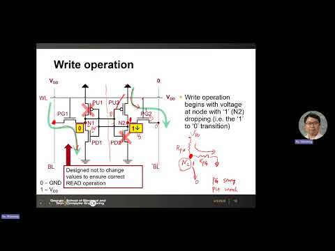
- SRAM writes proceed in sequence: the node storing 1 is pulled down first, then cross-coupled feedback raises the opposite node and completes the state change.
- Read stability is more demanding than hold stability because the selected pass gate raises the node storing 0, reducing the cell’s static noise margin.
- Increasing the pull-down-to-pass-gate beta ratio strengthens read stability, but requires a larger pull-down device and therefore increases SRAM cell area.
- Butterfly curves expose voltage margin and mismatch, whereas N-curves quantify tolerance to injected current and are practical for inline wafer testing.
- SRAM scaling slows at advanced nodes: representative cell area falls from about 0.1 μm² around 20–30 nm to roughly 0.02 μm² at 5 nm, with little further reduction reported.
Chapters
0:00
Estimating SRAM Read Latency from Bitline Capacitance
- During a read, the active pass gate and pull-down transistor create a path that discharges the bitline when the selected cell stores 0.
- The storage node rises slightly because of voltage division, while bitline capacitance includes wiring and attached transistor drain capacitances.
- Use Δt = CBL × ΔV / Iread; with 50 fF, a 100 mV sensing margin, and 10 μA, the estimated latency is 0.5 ns.
5:00
Preparing Complementary Bitlines for an SRAM Write
- A write driver forces complementary values onto BL and BLB; the example changes stored N1/N2 from 0/1 to 1/0.
- Unlike read precharge, write bias actively fixes one bitline at VDD and the other at ground.
- The two storage-node transitions do not occur simultaneously: the 1-to-0 transition starts the write.
10:00
Why the Stored 1-to-0 Transition Starts the Write
- The side intended to change from 0 to 1 initially resembles a read condition, so the read-stability design prevents its small voltage rise from flipping the cell by itself.
- On the side storing 1, the grounded bitline turns on the pass gate and pulls the storage node down against its pull-up transistor.
- The pull-down path must overcome the pull-up sufficiently to lower the node and initiate regeneration.
15:00
SRAM Write Timing and Pull-Up-to-Pass-Gate Strength
- Once the first node falls, cross-coupling turns on the opposite PMOS pull-up, which raises the other storage node and completes the flip.
- The write waveform therefore shows one node falling before the other rises, with their crossing point below VDD/2.
- The lecture defines γ as pull-up-to-pass-gate W/L and recommends γ ≤ 1; an NMOS pass gate can have greater drive than a PMOS pull-up even at equal W/L.
20:00
SRAM Array Peripherals: Precharge and Column Selection
- An SRAM array surrounds six-transistor cells with a wordline decoder, column mux, read sense amplifier, and write driver.
- The common three-transistor precharge circuit uses two PMOS devices to pull BL and BLB to VDD and a third to equalize them.
- A column mux selects the read or write path; the same three-device precharge topology is also used in DRAM, where the target is typically VDD/2.
25:00
Sense-Amplifier Latch Operation and Write Drivers
- A minimal SRAM sense amplifier is a cross-coupled inverter latch whose ground path is isolated by a sense-enable transistor.
- While disabled, the latch floats and its inputs can follow the small bitline difference; enabling it makes the lower-voltage side resolve to 0 and the other to 1.
- A write driver generates complementary bitline values and must be sized to drive bitline capacitance.
30:00
Read Timing: Waiting for the Sense Margin
- The wordline turns on first, allowing the selected cell to create a differential between the precharged bitlines.
- Sense-amplifier enable is delayed until the bitline difference reaches the required margin, typically about 100–200 mV.
- The resolved latch state is transferred to an output flip-flop and then to the data bus.
35:00
Butterfly Curves and Static Noise Margin
- Static stability analysis treats noise as persistent, making it a worst-case test of whether the SRAM cell retains its data.
- The butterfly curve overlays the voltage-transfer characteristics of the two cross-coupled inverters.
- Static noise margin is the side length of the largest square fitted between the curves; rotating the coordinates by 45° helps determine it.
40:00
Why Read Disturb Shrinks SRAM Noise Margin
- During a read, the selected pass gate and pull-down transistor raise the node storing 0 above ground through voltage division.
- That elevated low level distorts the butterfly curve and reduces the largest square, so read static noise margin is smaller than hold margin.
- For a read butterfly curve, sweep one storage-node voltage and solve the response using the pull-down, pass-gate, and pull-up transistor currents.
45:00
Using KCL to Construct the Read Butterfly Curve
- For the static read analysis, the wordline and bitline are held at VDD while the storage-node voltage is swept.
- At each point, Kirchhoff’s current law requires the pull-down, pass-gate, and pull-up currents to sum to zero.
- A stronger pull-down both steepens the transfer characteristic and keeps the disturbed low node closer to ground.
50:00
Beta Ratio, Supply Voltage, and Read Stability
- The beta ratio compares pull-down strength with pass-gate strength; increasing it improves read static noise margin.
- Simulation examples around a 20 nm process show that raising the ratio from 2 to 3 can improve margin by at least about 50 mV, at the cost of larger cell area.
- Lowering VDD saves power but also shrinks static noise margin, so designers must establish a minimum operating supply.
55:00
Write Static Noise Margin and Curve Separation
- Write stability focuses on the node intended to change from 1 to 0, where the bitline and pass-gate bias differ from the read case.
- The pull-up-to-pass-gate strength ratio affects how far the selected node can be pulled down toward 0.
- The write margin is determined by the smallest separation between the relevant curves: they must remain separated enough to avoid unwanted intersections while allowing the intended flip.
1:00:00
Measuring SRAM Stability with the N-Curve
- An on-chip test structure can sweep a voltage into a storage node and measure the current through the source, producing an N-shaped current-voltage curve.
- The voltage span between critical points characterizes voltage noise margin, while the maximum tolerable injected current defines static current noise margin.
- The curve records how much external current a node storing 0 can tolerate before the cell flips.
1:05:00
N-Curve Versus Butterfly-Curve Analysis
- Both methods describe SRAM stability, but the butterfly curve relates the two storage-node voltages while the N-curve relates an injected input voltage to current.
- Butterfly curves are useful for examining left-right transistor mismatch; the N-curve directly characterizes externally injected disturbances.
- N-curve measurements are convenient for wafer probing and inline process evaluation because voltage and current can be measured directly.
1:10:00
Measured SRAM Margins and Technology-Node Scaling
- Examples progress from roughly 250 mV static noise margin in 65 nm CMOS to about 200 mV at 32 nm and a lower-bound target near 100 mV at 10 nm.
- SRAM cell area is about 0.1 μm² around 20–30 nm, while a 5 nm example is about 0.02 μm²; the lecture notes little further SRAM scaling across newer nodes.
- Process variation creates distributions of butterfly curves, so designers assess the worst-case, smaller margin; limited SRAM scaling can make advanced-node cache implementations less attractive.
Summary, takeaways, and chapters were generated by AI from the video's transcript and may contain errors. The video belongs to its creator, Shimeng Yu.