Lecture 3 SRAM Part 1
 Watch on YouTube →
Overview
Shimeng Yu introduces SRAM as volatile, static memory that supports independent bit-level access, then explains the standard six-transistor (6T) cell and its hold, read, and write behavior. The lecture focuses on how cross-coupled inverters preserve data, how precharged bitlines and a sense amplifier enable reads, and why the pull-down-to-pass-gate strength ratio must exceed one to limit read disturb.
Key takeaways
- SRAM is volatile but requires no refresh, and its random-access operation allows individual bits to be read or written without block-level erase operations.
- A standard 6T SRAM cell stores complementary values on N1 and N2 using cross-coupled inverters, with two pass gates controlled by the word line.
- SRAM reads begin with both bitlines precharged to VDD and floating; the selected cell discharges one side slightly so a sense amplifier can resolve the data.
- Read access disturbs the internal node storing zero because current through the pass gate raises its voltage; the cell must preserve enough margin to avoid flipping.
- The pull-down-to-pass-gate strength ratio, defined by their W/L ratios, should exceed 1 so the pull-down holds the internal zero near ground during reads.
- The butterfly plot of the two inverter transfer curves shows two stable storage states and a metastable point, explaining both noise tolerance and the risk of state changes near instability.
Chapters
0:00
SRAM Properties and the Shift to On-Chip CPU Caches
- SRAM is static because it needs no periodic refresh, unlike DRAM, but it is volatile and loses its data when VDD is removed.
- Random access means individual SRAM bits can be read or written independently, unlike NAND flash operations that may require erasing an entire block.
- CPU caches evolved from off-chip SRAM to on-chip L1, L2, and L3 hierarchies; example 2011 capacities were 256 KB, 1 MB, and 8 MB.
- AMD's stacked V-Cache is a separate SRAM die bonded on top of a processor.
4:10
The Six-Transistor SRAM Cell and Its Cross-Coupled Inverters
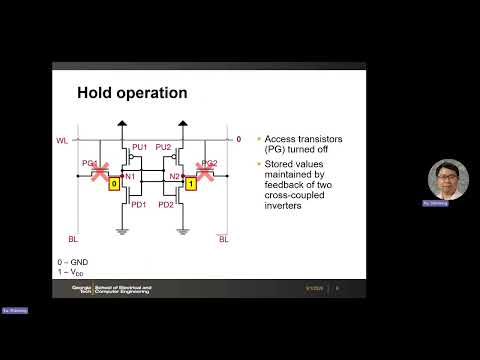
- A standard 6T cell uses two cross-coupled inverters to store complementary values at nodes N1 and N2.
- Two NMOS pass-gate transistors connect the storage nodes to complementary bitlines when the word line is asserted.
- The inverter transistors are called pull-down (PD) and pull-up (PU); the access transistors are pass gates (PG).
- With the word line low, the pass gates are off and the cross-coupled inverters maintain the stored state through positive feedback.
7:44
SRAM Hold, Read, and Write Operations
- In hold mode, VDD powers the cell while a low word line isolates N1 and N2 from the bitlines.
- For a read, both bitlines are precharged high and the selected word line connects the cell to them; the side storing zero discharges slightly.
- A sense amplifier detects the small voltage difference between the bitline and its complement and amplifies it into a digital output.
- For a write, external drivers set complementary bitline voltages, such as VDD and ground, and the asserted word line lets them flip the internal state.
13:19
Butterfly Curves Explain SRAM Hold Stability
- The two inverter voltage-transfer curves form a butterfly plot with two stable intersections for the stored states and one metastable intersection.
- A small disturbance at N1 changes N2 through one inverter, then feeds back through the other inverter.
- At either stable intersection, this feedback returns the cell toward its original state after a small noise disturbance.
- A disturbance near the metastable point can push the cell toward either stable state, depending on the direction of the perturbation.
18:09
Bitline Precharge and Read Disturb in a 6T Cell
- Before a read, both bitlines are precharged to VDD and then left floating; precharge is not a continuous connection or bias to VDD.
- When the selected word line turns on, current flows through the active pass gate and pull-down transistor, lowering one bitline by a small ΔV.
- The internal node storing zero rises slightly above ground as current passes through the pull-down device, creating a read disturb that must not flip the stored bit.
- The complementary bitline stays near VDD, allowing the sense amplifier to detect the developing voltage difference.
27:33
Sizing the Pull-Down-to-Pass-Gate Ratio and Recovering Read Data
- The read-stability design rule is to make the pull-down transistor stronger than the pass gate, so the internal zero node rises as little as possible.
- The SRAM beta ratio is defined as (W/L)PD ÷ (W/L)PG and should be somewhat greater than 1.
- During a read, the internal node disturbance should remain below roughly half of VDD, with additional margin for process variation.
- After sensing, the word line is closed and cross-coupled feedback restores the disturbed storage nodes; bitline capacitance accumulates along the array and can slow sensing.
Summary, takeaways, and chapters were generated by AI from the video's transcript and may contain errors. The video belongs to its creator, Shimeng Yu.