Lecture 3 DRAM Part 1
 Watch on YouTube →
Overview
Shimeng Yu explains how DRAM trades SRAM-like speed for much higher density, then connects the 1-transistor/1-capacitor cell to the architecture and timing limits of real memory systems. The lecture covers DIMM channels, ranks, banks, mats, DDR prefetch and bandwidth, memory product types including HBM, and the charge-sharing, sensing, and write-back sequence that makes a DRAM read destructive.
Key takeaways
- A DRAM read begins with a small charge-sharing signal, not a full logic-level voltage: precharging the bit line to VDD/2 lets stored 1s and 0s shift it in opposite directions for the sense amplifier.
- The 1T1C cell’s storage capacitance must be large relative to bit-line capacitance for reliable sensing, while its density requires a vertical cylindrical capacitor rather than flat plates.
- DRAM’s cell and array RC limits keep core access times near tens of nanoseconds; large gains in interface throughput instead come from DDR edge transfers, prefetch, faster I/O, and wider buses.
- A 64-bit DIMM operating at 1,600 Mb/s per pin provides 12.8 GB/s, illustrating that bandwidth is the per-pin rate multiplied by interface width and divided by eight to convert bits to bytes.
- HBM achieves high aggregate bandwidth and low transfer energy by placing a very wide interface close to the GPU; the lecture cites 1,024 pins for HBM3 and 2,048 for HBM4.
- Because sensing disturbs the storage node, the activated sense amplifier must restore the cell before the row is closed; this write-back is built into the DRAM read sequence.
Chapters
0:00
DRAM Versus SRAM: Density, Refresh, and Access Time
- DRAM is volatile dynamic memory: stored charge leaks, so cells require periodic refresh while powered.
- SRAM commonly serves as on-chip cache; DRAM is usually a separate off-chip chip, though packaging can bring it closer to a processor.
- A mainstream DRAM cell occupies about 6F², versus roughly 140–300F² for SRAM; DRAM access is typically 20–40 ns rather than around 1 ns or less.
- DRAM reads disturb stored data and require restoration; cell leakage must be exceptionally low, on the order of less than 1 fA per cell.
4:50
DIMM Channels, Ranks, and 64-Bit Data Transfers
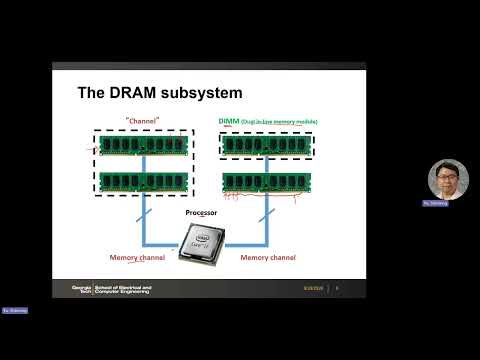
- A DIMM (dual in-line memory module) carries DRAM chips on a PCB that plugs into a desktop or workstation motherboard.
- Chips on a memory channel share its data bus; a conventional DIMM provides 64 data pins, transferring 64 bits in parallel per interface beat.
- A rank is a group of chips selected together; an example uses eight chips contributing 8 bits each to make a 64-bit channel transfer.
- A DIMM may have chips on both sides, forming two ranks, with selection circuitry choosing which rank drives the channel.
9:55
Banks, Row Buffers, and DRAM Mats
- A DRAM chip contains independently operable banks; the example uses eight banks and selects one for an access.
- Within a bank, activating a row copies its contents into the sense amplifiers, which serve as the row buffer.
- If the next request changes only the column address, data can come from the already-open row buffer; a different row requires another activation.
- A conceptual 16K-by-16K array contains 256 Mib; practical banks are divided into mats, such as 16-by-16 mats of 1K-by-1K cells, to control RC delay.
15:52
DDR Uses Both Clock Edges to Increase I/O Data Rate
- DDR means double data rate: its I/O transfers data on both rising and falling clock edges.
- In the example, a 200 MHz core and 200 MHz I/O clock yield 400 Mb/s per pin by using both edges.
- Later generations raise the I/O frequency: the DDR3 example uses an 800 MHz I/O clock for 1,600 Mb/s per pin.
- DRAM core frequency changes slowly because cell charge transfer is limited by RC behavior, while logic-based I/O circuitry can be scaled to run faster.
20:20
DDR Prefetch Converts Parallel Data into a Fast Serial Burst
- Prefetch gathers multiple bits in parallel inside DRAM, then serializes them through the I/O at a higher rate.
- The DDR3 example prefetches eight bits in one core-clock interval and sends them out sequentially over the interface.
- At 1,600 Mb/s per pin across 64 data pins, the example DIMM reaches 12.8 GB/s: 1,600 Mb/s × 64 ÷ 8.
- Bandwidth depends on both per-pin data rate and pin count; HBM gains bandwidth chiefly through a much wider interface, around 1,024 pins in the example.
25:22
DRAM History and the Slow Growth of Core Access Speed
- IBM engineer Robert Dennard proposed representing data with charge stored on capacitors, the principle behind DRAM.
- The first available DRAM chip, introduced in 1973, used three transistors; the dedicated-capacitor 1T1C cell became the desired density-oriented design.
- The lecture contrasts a 12 V, roughly 300 ns early product with modern access times near 30 ns: core access improved only about tenfold over more than five decades.
- DRAM data rates grew by orders of magnitude mainly through I/O improvements rather than a comparable increase in intrinsic cell speed.
29:16
DRAM Process Nodes and Product Families
- The lecture places current DRAM production around the 1C node, roughly 12 nm in critical dimension, after the 1X, 1Y, 1Z, 1α, and 1β naming sequence.
- A contemporary DRAM die is described as roughly 32 Gb, or 4 GB, with DDR supply voltage near 1.1 V.
- DDR DIMMs primarily serve as server and host memory; LPDDR targets mobile devices with lower power and often package-level integration.
- GDDR serves high-performance graphics and some AI workloads, while HBM is packaged alongside a GPU for a much wider, shorter-reach interface.
33:06
DDR, LPDDR, and GDDR Trade Cost, Power, and Speed
- The lecture cites a first-generation DDR5 example from SK hynix with 16 GB capacity, 32 banks, and 6.4 Gb/s per pin.
- Cost-focused DDR favors large mats and banks where timing permits, reducing area overhead while respecting bit-line and word-line RC limits.
- LPDDR5 emphasizes battery life through low leakage, infrequent refresh, and simpler I/O; the cited Samsung example reaches 8 Gb/s per pin.
- GDDR6 prioritizes performance: the cited Micron example reaches 22 Gb/s per pin and uses shorter bit lines, accepting additional area and cost.
37:52
HBM Bandwidth Comes from a Wide Interface
- Per-pin rates and aggregate bandwidth are distinct: aggregate bandwidth equals data rate per pin multiplied by the number of I/O pins.
- One HBM stack can provide about 1–2 TB/s in the cited comparison, substantially exceeding conventional DDR bandwidth.
- HBM3 uses 1,024 I/O pins in the example, while the lecture notes HBM4 moving to 2,048; parallel width, not exceptionally high per-pin speed, drives the bandwidth.
- The HBM interface’s short connection to the GPU also lowers energy per transferred bit compared with off-package memory links.
42:23
DRAM Market Leaders and HBM Capacity Pressure
- The principal DRAM suppliers identified are Samsung, SK hynix, and Micron, with China’s CXMT described as a rapidly developing competitor.
- The lecture links SK hynix’s market-share gains to its early HBM position and supply relationships with Nvidia.
- HBM’s strong demand and profitability encourage vendors to allocate wafer capacity to HBM, tightening supply for DDR and LPDDR.
- New fabrication plants take years to build, so adding wafer capacity cannot immediately resolve a memory shortage.
46:36
The 1T1C Cell and Its Vertical Capacitor
- A DRAM cell has one access transistor controlled by the word line and one storage capacitor connected between the storage node and a common plate.
- The transistor connects the storage node to the bit line; a charged storage node represents 1, while removing its charge represents 0.
- To fit useful capacitance into a dense cell, the capacitor is built vertically as a cylindrical or U-shaped structure with inner and outer electrodes.
- The cell array is integrated with peripheral DRAM logic, including decoders, sense amplifiers, and I/O circuitry.
52:21
Charge Sharing Produces the DRAM Read Signal
- Before sensing, the bit line is precharged to half of VDD; activating the word line connects it to the cell’s storage node.
- For a stored 1, charge flows from a storage node initially near VDD into the half-VDD bit line, shifting the bit-line voltage upward; a stored 0 shifts it downward.
- Charge conservation gives a signal magnitude proportional to ½VDD divided by 1 + CBL/CS, where CBL is bit-line capacitance and CS is cell capacitance.
- A larger storage capacitance relative to bit-line capacitance increases the sense margin, explaining the need for the cell’s tall capacitor.
1:01:00
RC Delay Limits Charge Sharing and Core Speed
- Charge sharing takes time because the access transistor contributes channel resistance between the storage capacitor and bit line.
- The effective capacitance in the charge-transfer path is the series combination CS × CBL / (CS + CBL).
- Lower access-transistor resistance speeds sensing, but the cell still needs a large CS to preserve signal margin.
- These capacitance and resistance requirements help explain why DRAM core timing is difficult to improve even as I/O rates rise.
1:03:12
Sense-Amplifier Latching Restores Read Data
- Charge sharing leaves the storage-node voltage below its original value, so a DRAM read must write the sensed value back into the cell.
- The sense amplifier is a cross-coupled inverter latch connected to complementary bit lines, with pull-up and pull-down devices controlled by sense enable.
- For a stored 1, the small positive bit-line deviation makes the latch drive one line toward VDD; because the word line remains active, that voltage recharges the cell.
- The word line may use an elevated VPP level to strengthen the access transistor, and a negative VBB level while inactive to reduce leakage.
1:09:55
Precharge, Column Selection, and DRAM Timing Parameters
- An equalizer precharges complementary bit lines to half VDD before sensing; after the sense amplifier resolves the data, a column-select signal connects it to the data bus.
- A valid signal must exceed sense-amplifier mismatch, process variation, and thermal noise; the lecture gives roughly 100 mV as a representative threshold.
- The timing discussion identifies tRCD as row-to-column delay, tRC as the row-cycle interval, tWR as write recovery, and tRP as precharge time.
- Typical examples include a 40–50 ns row cycle and about 15 ns for tRCD; column-select pulses around 2.5 ns correspond to a roughly 200 MHz core cadence.
Summary, takeaways, and chapters were generated by AI from the video's transcript and may contain errors. The video belongs to its creator, Shimeng Yu.