Lecture 2 CMOS Review and Scaling Part 2
 Watch on YouTube →
Overview
CMOS scaling has shifted from planar transistors toward 3D gate structures: strained silicon and high-k metal gates improved mobility and drive current, FinFETs strengthened gate control, and gate-all-around nanosheets enable further scaling. Shimeng Yu explains CFET stacking as a potential next step, then connects transistor scaling to foundry and memory markets, semiconductor business models, and changes in company rankings.
Key takeaways
- CMOS performance improvements come from both carrier mobility and gate capacitance: strained silicon boosts mobility, while high-k dielectrics raise Cₒₓ and support higher drive current.
- FinFETs control channels from three sides, whereas gate-all-around nanosheets wrap the channel on four sides and can be stacked vertically.
- CFETs could cut inverter area by about 50% by stacking NMOS and PMOS, but heat concentration, interconnect parasitics, and integration complexity remain significant challenges.
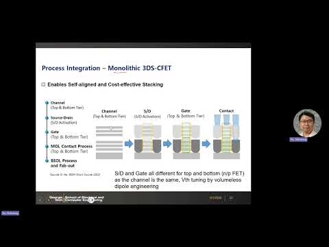
- In monolithic CFETs, shared channel material makes gate-stack work-function and dipole engineering important tools for setting NMOS and PMOS threshold voltages.
- The lecture’s cited 2026 forecast assigns $600 billion of a $1 trillion semiconductor market to memory, reflecting AI infrastructure demand for DRAM and flash.
- Logic scaling is better tracked through contacted poly pitch, M1 pitch, and standard-cell height than through node names, which do not directly specify transistor dimensions.
Chapters
0:00
CMOS Scaling: Strained Silicon and High-k Metal Gates
- At the 90 nm node, strained silicon used source-and-drain stress to alter silicon’s band structure and improve carrier mobility, particularly for PMOS.
- At 45 nm, high-k metal gates replaced the traditional polysilicon and silicon-dioxide stack; hafnium-based dielectrics can have roughly four to five times silicon dioxide’s dielectric constant.
- Higher mobility and gate capacitance increase drive current; the saturation-current relationship makes both μ and Cₒₓ key performance factors.
5:00
FinFETs and Gate-All-Around Nanosheet Transistors
- FinFETs arrived around the 22 nm node, moving from planar channels to a 3D fin that the gate controls from three sides.
- Gate-all-around nanosheets extend that control around four sides of a horizontal silicon channel and can be stacked in multiple tiers.
- Samsung calls its implementation MBCFET, Intel uses the term RibbonFET, and nanosheet designs are associated with leading 2 nm- and 18A-class processes.
- Node names are marketing labels, not literal gate lengths; Yu notes that gate lengths remain around 15 nm even as some nanosheet and gate-stack dimensions approach a few nanometers.
10:00
CFETs: Vertically Stacking NMOS and PMOS
- Complementary FETs (CFETs) place NMOS and PMOS devices vertically rather than side by side, potentially reducing inverter footprint by roughly 50%.
- Intel showed an early CFET demonstration in a 2020 paper; Intel, TSMC, and Samsung have reported research in this area.
- The approach is presented as a possible future technology, with active research still needed before production.
- Vertical integration can concentrate heat, so thermal self-heating and heat dissipation remain unresolved concerns.
14:00
Monolithic CFET Integration and Threshold-Voltage Tuning
- In monolithic integration, epitaxial silicon and silicon-germanium layers are grown in alternating stacks; selectively etching away the silicon-germanium releases thin silicon nanosheets.
- NMOS and PMOS can share the same channel material, so gate-stack work-function engineering becomes important for setting their different threshold voltages.
- Because the gate region is extremely small, volumeless dipole engineering can use an approximately atomic-scale interfacial layer to shift the built-in potential and tune threshold voltage.
- Yu frames the detailed integration process as context about industry research rather than material required for homework or exams.
19:00
Sequential CFET Stacking: Wafer Bonding Trade-offs
- Sequential integration fabricates a bottom transistor tier, bonds a separate wafer or transferred layer on top, and then fabricates the upper tier.
- Unlike monolithic integration, the two tiers can be optimized separately—for example, using different channel materials for NMOS and PMOS.
- Wafer bonding introduces alignment demands and can leave a greater distance between tiers, increasing interconnect parasitic resistance and capacitance.
- The sequential and monolithic approaches are both under research as ways to scale logic vertically.
25:00
Memory’s Growing Share of the Semiconductor Market
- Yu’s 2020 comparison puts DRAM and flash at about 27% of semiconductor revenue, or roughly $126 billion; embedded SRAM is excluded because it is integrated into processors and accelerators.
- A 2026 analyst forecast cited in the lecture projects about $1 trillion in total semiconductor revenue and $600 billion in memory revenue, driven by AI data-center infrastructure.
- Samsung, SK hynix, and Micron are highlighted as major beneficiaries of demand for DRAM and flash.
29:00
Foundries, Fabless Designers, IDMs, and EDA Vendors
- TSMC is described as holding about 70% of foundry business by wafer capacity and revenue; other foundries include GlobalFoundries and Japan’s developing Rapidus.
- Hyperscalers including Google, Meta, Microsoft, and Amazon increasingly work with ASIC designers such as Broadcom and Marvell on custom chips.
- Intel and Samsung combine design and manufacturing as integrated device manufacturers; Intel’s IDM 2.0 effort also seeks external foundry customers.
- The lecture notes that Intel has outsourced some high-end processor manufacturing to TSMC amid yield challenges, while Synopsys, Cadence, and Siemens EDA are key design-tool vendors.
37:00
Semiconductor Revenue Rankings: Nvidia’s Rise and Industry Shifts
- Qualcomm entered the top ten around 2010 as smartphones expanded, while Nvidia first appeared in the top 20 around 2014 and reached the top ten by 2018.
- By 2020, three of the top five companies were memory makers; in 2023, Nvidia rose into the top three and TSMC ranked first in the figures discussed.
- Yu describes long-term declines among several Japanese semiconductor companies and notes Micron’s 2014 acquisition of Japan’s Elpida.
43:00
Scaling Metrics: Standard-Cell Height and Future CFETs
- For logic, contacted poly pitch and M1 pitch are more informative scaling measures than the marketed node name.
- Reducing standard-cell height improves integration density; CFETs could shrink it by folding NMOS and PMOS devices into a vertical stack.
- For DRAM and flash, feature size and half-pitch are more relevant measures, while the logic roadmap proceeds from FinFETs to nanosheets and potentially CFETs.
Summary, takeaways, and chapters were generated by AI from the video's transcript and may contain errors. The video belongs to its creator, Shimeng Yu.