EE 330 Lecture 2026 10 13 Ch5 MOS#5
 Watch on YouTube →
Overview
Chapter 5 applies MOSFET operating-region tests and current equations to NMOS, PMOS, and complementary MOS circuits, emphasizing that assumed saturation must be verified using terminal voltages. Worked examples calculate bias voltages and currents, recover unknown resistor values, and find maximum drain resistance before a transistor enters triode operation; the final cases compare saturation-based and triode-based solutions for inputs of 0 and ±2.5 V.
Key takeaways
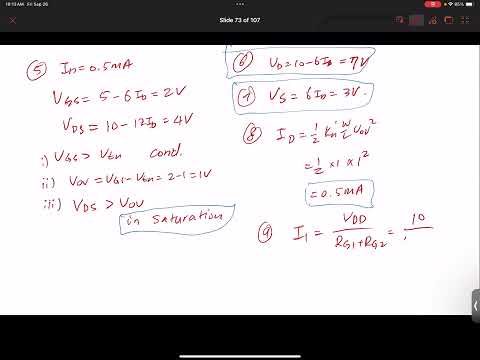
- For the NMOS example with VDD = 10 V, 10 kΩ gate-divider resistors, and 6 kΩ source and drain resistors, the consistent solution is ID = 0.5 mA, VGS = 2 V, and VDS = 4 V; VDS > VOV = 1 V confirms saturation.
- The saturation boundary provides a direct maximum-resistance calculation: the NMOS circuit in Exercise 5.12 permits RD up to 12 kΩ, while the PMOS circuit in Example 5.7 permits RD up to 8 kΩ.
- Exercise 5.13 demonstrates reverse bias design: measured node voltages and ID = 0.32 mA produce RD = RS = 5 kΩ and a gate divider of RG1 = 1.6 MΩ and RG2 = 3.4 MΩ.
- MOSFET region assumptions must be checked after solving; in Example 5.8, the NMOS saturation estimate violates its voltage condition, so the triode equation is required.
- For matched complementary devices at zero input, symmetry supports a zero-output, zero-current operating point; nonzero ±2.5 V inputs activate opposite transistor types in the analyzed circuits.
Chapters
0:00
Chapter 5 Design Examples and the MOSFET Analysis Workflow
- The lecture continues Chapter 5 with circuit examples, using repeated calculations to build MOSFET design and analysis skills.
- The first circuit includes gate-divider resistors and source and drain resistors; given parameters include VDD = 10 V, VTN = 1 V, K = 1 mA/V², and λ = 0.
3:00
Example 5.6: Find the NMOS Gate Bias with a Divider
- With IG = 0, RG1 and RG2 are in series and form a voltage divider at the gate.
- For RG1 = RG2 = 10 kΩ and VDD = 10 V, the gate voltage is VG = 5 V and the divider current is 0.5 mA.
- The analysis distinguishes VG from VGS: the source resistor means VGS = VG − VS, not simply VG.
6:00
Example 5.6: Solve the NMOS Current and Verify Saturation
- With RD = RS = 6 kΩ, ID = IS and the node voltages satisfy VD = 10 − 6ID and VS = 6ID, using ID in milliamps.
- Assuming saturation gives ID = ½K(VGS − VTN)², with VGS = 5 − 6ID; the physically valid quadratic root is ID = 0.5 mA.
- The resulting VGS = 2 V, VDS = 4 V, VD = 7 V, and VS = 3 V; since VDS exceeds VOV = 1 V, saturation is confirmed.
14:11
Exercise 5.12: Find the Maximum NMOS Drain Resistance
- Increasing RD lowers VD and VDS, while the previously solved bias current remains ID = 0.5 mA.
- At the saturation boundary, VDS = VOV = 1 V; with VS = 3 V, the drain must remain at or above 4 V.
- The boundary gives RD ≤ 12 kΩ, the maximum drain resistance that keeps the NMOS in saturation.
19:09
Exercise 5.13: Reconstruct Bias Values from Given Node Voltages
- Given VDD = 5 V, VD = 3.4 V, VS = 1.6 V, ID = 0.32 mA, and a 1 μA gate-divider current, first find VDS = 1.8 V.
- The NMOS current equation gives VOV = 0.8 V; because VDS > VOV, the saturation assumption is valid.
- With VTN = 1 V, VGS = 1.8 V and VG = VGS + VS = 3.4 V.
23:00
Exercise 5.13: Calculate the Drain, Source, and Gate Resistors
- The resistor drops give RD = (5 − 3.4 V)/0.32 mA = 5 kΩ and RS = 1.6 V/0.32 mA = 5 kΩ.
- The 5 V divider supply and 1 μA current require RG1 + RG2 = 5 MΩ.
- Since VG = 3.4 V, the divider values are RG2 = 3.4 MΩ and RG1 = 1.6 MΩ.
27:58
Example 5.7: Set Up the PMOS Saturation-Boundary Problem
- For the PMOS circuit, use source-referenced voltages VSG and VSD and the magnitude |VTP| = 1 V.
- The given drain current is 0.5 mA, KP = 1 mA/V², λ = 0, and the source is at 5 V.
- Increasing RD lowers the drain voltage and VSD, so the task is to find the gate bias and maximum RD that preserve saturation.
32:10
Example 5.7: Determine PMOS Overdrive and Gate Bias
- Using the saturation current equation, ID = ½KP(VSG − |VTP|)², the specified 0.5 mA current gives an overdrive voltage of 1 V.
- Therefore VSG = 2 V and the gate voltage is VG = 5 − 2 = 3 V.
- The gate-divider ratio must satisfy RG2/(RG1 + RG2) = 3/5; multiple resistor pairs can meet this ratio.
37:34
Example 5.7: Find the PMOS Maximum Drain Resistance
- PMOS saturation requires VSD ≥ VOV; at the boundary, VSD = 1 V.
- With the source at 5 V and ID = 0.5 mA, the resistance drop must be no more than 4 V.
- Thus RD ≤ 4 V/0.5 mA = 8 kΩ; the analysis again assumes a region and checks its voltage condition.
39:25
Exercise 5.14: Analyze a Matched NMOS–PMOS Pair
- The complementary circuit uses matched NMOS and PMOS devices, threshold magnitudes of 1 V, λ = 0, and a 10 kΩ load.
- The input is evaluated at 0 V and at ±2.5 V; each case requires determining which transistor is off, saturated, or in triode.
- Matched devices provide symmetry that helps analyze the zero-input operating point.
47:05
Exercise 5.14: Zero Input and the Positive-Input Case
- At Vi = 0 V, the matched, symmetric circuit has equal device conditions, yielding an output of 0 V and no load current.
- For Vi = +2.5 V, the NMOS conducts while the PMOS is treated as off.
- Solving the NMOS saturation equation together with the 10 kΩ load relation gives an output near 1.104 V and current near 0.104 mA.
56:58
Exercise 5.14: Negative Input and Complementary Response
- At Vi = −2.5 V, the PMOS conducts and the NMOS is treated as off, reversing the positive-input operating pattern.
- The same load-based current analysis gives a PMOS current near 0.104 mA.
- The response is described as approximately symmetric with the positive-input case.
1:05:51
Example 5.8: Start the Three-Input Operating-Region Cases
- The next complementary MOS circuit uses K values of 1, threshold magnitudes of 1 V, and λ = 0, with Vi tested at 0 and ±2.5 V.
- At zero input, matched-device symmetry gives an output of 0 V and zero current.
- For Vi = +2.5 V, the PMOS is off and the NMOS turns on; the initial saturation assumption must be checked against the resulting output.
1:08:27
Example 5.8: Reject the NMOS Saturation Assumption
- With Vi = +2.5 V, the NMOS has VGS = 5 V and an overdrive of 4 V.
- A saturation-based estimate produces an output that is too large to satisfy the assumed region conditions.
- The inconsistency shows that the NMOS must instead be analyzed in triode.
1:11:40
Example 5.8: Use the Triode Equation for the ±2.5 V Cases
- In triode, the current uses the channel equation proportional to (VGS − VTN)VDS − ½VDS²; for small VDS, the quadratic term can be comparatively small.
- Combining the triode equation with the 10 kΩ load relation gives an output magnitude near 2.44 V and current near 0.244 mA for the conducting-device cases.
- The final operating-region conclusion is triode for the nonzero-input cases, rather than saturation.
Summary, takeaways, and chapters were generated by AI from the video's transcript and may contain errors. The video belongs to its creator, Wireless Power Transfer.