ECE1756_lecture4_part2_2026_compute_device_comparison
 Watch on YouTube →
Overview
Vaughn Betz compares FPGAs, CPUs, GPUs, DSPs, and ASICs using peak compute, power, bandwidth, area, and delay, emphasizing that peak figures are useful first-order estimates but depend heavily on workload and assumptions. The comparisons show FPGA strengths in small-integer efficiency and high-speed networking, while ASICs can be far more efficient and processor-style programmability can be costly; FPGAs often occupy the practical middle ground when flexibility and streaming-style parallelism matter.
Key takeaways
- An FPGA peak-throughput estimate based on one compiled unit scaled to 85% utilization can be useful, but assuming unchanged frequency across hundreds of copies ignores placement difficulty and routing congestion.
- The paper's FPGA power estimates likely overstate consumption because they assume 100% signal toggling; 50% is a more reasonable initial activity estimate for arithmetic datapaths.
- FPGAs excel at narrow integer workloads: the analyzed devices reach about 10× GPU and 5× CPU compute per watt for 16-bit integer operations, while GPUs retain higher total throughput and DRAM bandwidth.
- FPGA area overhead varies substantially with resource mix: roughly 20–25× for logic-heavy designs after accounting for ASIC routability, but around 4× when the FPGA's logic, RAM, and DSP resources are all used.
- FPGA-to-ASIC delay remains around 3× in the cited study even when hard blocks are added, because the critical path often stays in programmable logic.
- For regular, parallel workloads, streaming hardware can beat processor-style execution by large margins; SIMD narrows the processor gap, but the cited FPGA study still reports roughly 900× worse area-delay for an eight-lane vector processor than streaming units.
Chapters
0:00
Peak Analysis as a First-Pass Device Comparison
- Betz introduces a research paper that compares FPGAs, DSPs, GPUs, and CPUs without implementing hundreds of full applications on every device.
- The analysis focuses on compute density, compute per watt, on-chip and off-chip memory bandwidth, and connectivity bandwidth.
- Peak analysis is a practical starting point, not a performance guarantee; the paper's device generations are dated, but its comparison method remains useful.
2:43
Estimating FPGA Peak Throughput with Replicated MAC Units
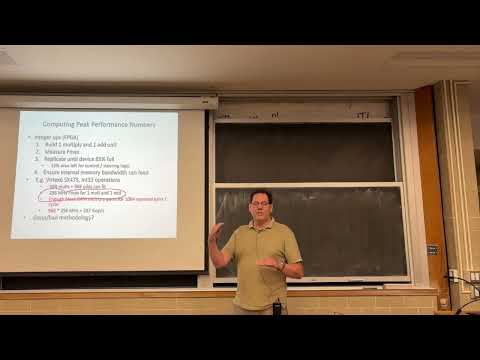
- Because FPGA vendors do not publish a single peak-performance figure, the study builds integer multiply-and-add units and replicates them until estimated logic use reaches 85%.
- For a Xilinx Virtex-6 example, the 32-bit design fits 968 multipliers and 969 adders, with a measured single-unit frequency of 296 MHz.
- The estimate checks whether block RAM can feed the units; more than 1,000 operand pairs can be supplied per cycle, so compute capacity—not block-RAM bandwidth—is the assumed limit.
- Multiplying 968 units by the assumed frequency gives an estimated peak of 287 GOPS.
6:45
Why Replicated FPGA Peak Estimates Are Optimistic
- The method scales resource use linearly from one compiled unit and assumes frequency remains constant as hundreds of copies are added.
- FPGA routing congestion and harder place-and-route problems can reduce frequency as utilization rises, particularly near 90–100% occupancy.
- The study leaves 15% of logic unused for control and muxing, but that margin is a rule of thumb rather than a rigorous application-independent value.
- Betz notes that fully compiling a near-capacity design could take hours; the estimate is still informative, but likely optimistic.
13:25
How CPUs, GPUs, DSPs, and FPGAs Scale with Operand Type
- CPU SIMD width favors 16-bit integers over 32-bit integers on some processors, while GPUs generally deliver strong single-precision floating-point throughput.
- DSPs have lower absolute peak throughput than GPUs, but their design targets power-efficient signal processing rather than maximum raw performance.
- FPGAs benefit strongly from narrower operands: 16-bit integer performance exceeds 32-bit performance, and 8-bit data would improve packing further.
- Floating-point hardware costs more FPGA resources; double precision is especially demanding, so it warrants careful device-selection analysis.
16:35
Dynamic Power, Toggle Activity, and the FPGA Power Estimate
- Dynamic CMOS power follows approximately P = ½CV²fα, where capacitance, voltage, clock frequency, and signal activity determine switching power.
- A 50% toggle rate is a reasonable first estimate for arithmetic datapaths with changing data; control logic may be closer to 10%.
- The study assumes 100% signal toggling for FPGA power, which Betz considers unusually high and likely to overstate FPGA consumption.
- Static power varies less with the workload, while dynamic power is more affected by the design and can be estimated more accurately using simulation.
24:06
Process Nodes and FPGA Compute per Watt
- The study finds that Virtex-7 at 28 nm is more power-efficient than Virtex-6 at 40 nm, with a similar trend in Altera's 28 nm and 40 nm devices.
- Smaller transistors and shorter wires reduce capacitance, lowering dynamic power; modest voltage reductions can contribute as well.
- Leakage becomes harder to control at newer nodes, but for heavily active compute workloads, dynamic-power improvements can outweigh increased static-power challenges.
- For 16-bit integer operations, the analyzed FPGAs reach roughly 10× the compute per watt of a GPU and 5× that of a CPU; FPGA and GPU floating-point efficiency is closer, though FPGA total throughput is lower.
31:17
DRAM Bandwidth Versus Networking Bandwidth
- GPUs tend to provide the highest external-memory bandwidth, DSPs rely more on data already brought on chip, and CPUs fall between them.
- In the paper's comparison, GPUs have about 3× the FPGA DRAM bandwidth, while FPGAs have about 10× the bandwidth for networking and other I/O.
- High-bandwidth memory uses stacked DRAM connected through a silicon interposer; GPUs often deploy more of it, although FPGAs can also use the technology.
- The difference reflects target markets: GPUs prioritize moving large data volumes, while FPGAs commonly devote I/O resources to Ethernet and other high-speed links.
37:39
FPGA-to-ASIC Area Gap: Logic and Hard Blocks
- A study associated with Jonathan Rose compares FPGA implementations in Quartus with standard-cell ASIC implementations using a conventional synthesis and place-and-route flow.
- For logic-only designs, FPGA area is reported at about 35× ASIC area in the same process generation, including programmable routing overhead.
- Adding DSP and RAM blocks narrows the gap because hardened FPGA blocks resemble ASIC structures more closely: reported ratios fall to about 25× for logic plus multipliers and 18× for logic, multipliers, and RAM.
- If a design is adapted to use all available FPGA resource types, the estimated area gap can fall to about 4×.
46:33
Benchmark and Floorplan Caveats in Area Comparisons
- The benchmark set is small and unrepresentative in important ways: most designs are tiny, and almost no modern complete designs lack memory.
- The study's ASIC floorplans can pack small designs unusually tightly; larger ASIC designs often need routing space, with roughly two-thirds placement density offered as a practical rule of thumb.
- Accounting for more realistic ASIC routability reduces the logic-only comparison from 35× to a still-large estimated range of roughly 20–25×.
- Area ratios depend strongly on what the FPGA uses: programmable logic has the largest overhead, while RAM and DSP blocks are much closer to their ASIC counterparts.
49:04
Why Hard Blocks Improve Area More Than Delay
- The measured FPGA-to-ASIC delay gap is about 3× for logic-only designs and remains similar when RAM and DSP blocks are included.
- A DSP block can shrink multiplier area substantially, but it may not improve the design's clock period if near-critical paths remain in programmable logic.
- Area sums contributions across the whole design, whereas delay is set by the worst path; improving only some paths may therefore have little timing impact.
- To realize larger speedups from hard blocks, designers may need to re-optimize or re-pipeline the surrounding logic.
54:02
Area-Delay Product and the ASIC Efficiency Advantage
- Area-delay product approximates the inverse of throughput per unit silicon: halving area allows twice as many copies, while halving delay permits twice the clock rate.
- The older study's FPGA-to-ASIC area-delay gap ranges from about 12× to 60×, depending on how much the design uses FPGA hard blocks.
- A later CNN-accelerator comparison reports an 8× area gap and a 4× delay gap, or about 32× area-delay, against a fixed-function ASIC.
- That ASIC comparison assumes one non-programmable model; adding ASIC programmability to manage changing workloads would reduce some of the apparent efficiency advantage.
58:52
Scalar and SIMD Processors Versus Streaming Hardware
- A separate study implements a scalar processor and dedicated streaming units on the same FPGA to isolate the cost of the programming model.
- The scalar processor is 432× slower and 6.7× larger than the streaming hardware, producing an approximately 2,900× area-delay disadvantage on the tested workloads.
- Adding SIMD makes the processor 36× larger but only 25× slower, reducing its area-delay disadvantage to roughly 900×.
- An eight-lane SIMD width is the reported sweet spot for those applications, though streaming hardware remains substantially more efficient.
1:01:16
Choosing Between ASICs, FPGAs, and Programmable Processors
- A fixed-function ASIC with streaming hardware offers the best efficiency when cost, development time, and confidence in a stable design are not constraints.
- FPGAs trade some ASIC efficiency for reconfigurability; designs using many hard blocks can approach a roughly 12× area-delay penalty, while soft-logic-heavy designs can be closer to 60×.
- When custom fabrication is impractical, an FPGA can outperform even a throughput-oriented vector processor on highly regular, parallel workloads.
- Betz cautions against stacking two kinds of programmability—such as running the main design as a processor on an FPGA—when direct FPGA streaming hardware is feasible.
1:08:16
Time-to-Market, Production Volume, and FPGA Use in Telecom
- Cellular infrastructure often uses a mix of ASICs, FPGAs, and DSPs because evolving standards make time to market and the ability to debug early systems valuable.
- A late 5G product can lose market position, so spending engineering effort on a 5G ASIC may be unattractive if it delays a 6G design.
- At volumes such as tens of millions of tightly power-constrained phones, ASIC economics are compelling; lower-volume, expensive base-station equipment has a more complex trade-off.
- Betz describes FPGA and ASIC competition at multiple points in telecom systems, with the best choice depending on volume, timing, and workload.
1:12:34
Workload Caveats and Why SIMD Is the Relevant Processor Baseline
- The streaming-hardware study's integer benchmarks range from 1-bit to 32-bit operands; its results do not automatically generalize to floating-point or wider-operand applications.
- Very narrow datapaths make processor control overhead look especially costly because a processor's wider datapath is underused.
- SIMD processor results are more relevant than scalar results for current device selection because most commonly available processors include SIMD instructions.
- Streaming hardware's strongest advantage applies to regular workloads with abundant parallelism and limited control flow, not every application.
Summary, takeaways, and chapters were generated by AI from the video's transcript and may contain errors. The video belongs to its creator, Vaughn Betz.